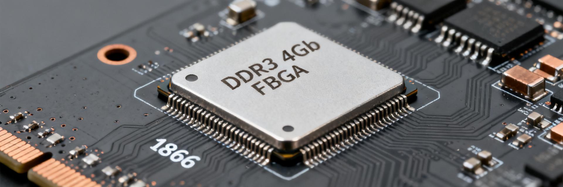
• تقرير فني شامل: H5ANAG8NCJR-XNC 16 جيجابت DDR4

    يشير تحليل السوق إلى وجود طلب مستمر على خيارات ذاكرة DRAM ذات الموثوقية العالية والفعالية من حيث التكلفة عبر كل من الأنظمة المدمجة والبنى القديمة. يعمل هذا التقرير كدليل هندسي مفصل لتقييم وتوجيه وتطبيق شريحة الذاكرة H5ANAG8NCJR-XNC بسعة 16 جيجابيت من نوع DDR4 SDRAM. 1 — الخلفية ونظرة عامة على المنتج بنية الجهاز والتنظيم المنطقي يُعد جهاز H5ANAG8NCJR-XNC شريحة ذاكرة أحادية عالية الكثافة بسعة 16 جيجابيت من نوع DDR4 SDRAM، وهي منظمة منطقياً كصفوف بمصفوفة 2G x8. داخلياً، تنقسم مصفوفة الذاكرة إلى مجموعات بنوك متعددة (Bank Groups) لتحقيق السرعة المثلى لخطوط المعالجة المترابطة (Pipelining). تتعامل الأنظمة على مستوى اللوحة مع الشريحة كعنصر قياسي بعرض 8 بت، مما يتيح للمصممين تجميع تكوينات رتب مرنة (على سبيل المثال، بناء قناة بعرض 64 بت باستخدام ثماني شرائح x8 متوازية). التنظيم عرض البت تكوينات الوحدات المستهدفة 2G x8 x8 رتبة فردية بـ 8 شرائح (8 جيجابايت)، رتبة مزدوجة بـ 16 شريحة (16 جيجابايت) 4G x4 (متغير منطقي) x4 وحدات مدمجة عالية الكثافة متعددة الرتب ذات مخزن مؤقت للمسجلات خاصة بالمؤسسات التطبيقات المستهدفة وسياق السوق يلبي هذا الجهاز ذو الكثافة البالغة 16 جيجابيت بشكل كبير احتياجات بطاقات خطوط أجهزة الاتصالات، ومتحكمات الأجهزة المدمجة، ودورات ترقية الخوادم القديمة، وبنى الحوسبة الصناعية الخالية من المراوح. إن الانتقال إلى تصميم بسعة 16 جيجابيت لكل قالب يقلل بشكل مباشر من حجم اللوحة، ويحد من ازدحام مسارات التوصيل مقارنة باستخدام شرائح متعددة بسعة 8 جيجابيت، ويحافظ على دورات حياة المنصة دون الحاجة إلى ترقيات كاملة للنظام على شريحة (SoC). 2 — المواصفات الكهربائية الرئيسية وتفاصيل الحزمة المواصفات الكهربائية الأساسية ومعلمات التوقيت تتبع معلمات تشغيل الجهاز إرشادات JEDEC DDR4 القياسية، حيث تعمل على خط جهد نواة اسمي Vdd يبلغ 1.2 فولت. وتتدرج فئات سرعة التشغيل لتصل إلى DDR4-3200، مما يتيح أداءً قوياً في ظل تكوينات المعالجة القصوى. تتراوح ملفات تعريف زمن انتقال CAS عادةً من CL14 إلى CL22 اعتماداً على تصنيف السرعة المحدد للمتحكم. المعلمة القيمة النموذجية ملاحظة / شرط الاختبار Vdd (النواة) 1.2 V ± 0.06V نطاق الإمداد القياسي وفقاً لمواصفات JEDEC معدل البيانات حتى 3200 MT/s يعتمد على تكوين متحكم النظام tCL (زمن انتقال CAS) 14–22 دورة يتم تحسينه بواسطة دورة تدريب البرامج الثابتة نطاق درجة حرارة التشغيل من 0 درجة مئوية إلى 85 درجة مئوية قابل للتمديد إلى 95 درجة مئوية مع مضاعفة معدلات التحديث الحزمة، وتوزيع الأطراف والاعتبارات الفيزيائية يتوفر الجهاز في مساحة حزمة FBGA قياسية، وهو يوازن بين الاستقرار الهيكلي ومسارات الهروب لتوجيه الأسلاك. يجب على فرق تخطيط الأجهزة إيلاء اهتمام بالغ لمنصات التوصيل المستهدفة، ومطابقة أبعاد المسارات مع مصفوفات الكرات عالية الكثافة، وتوفير خلوص مادي مناسب تحتها للتخلص من التداخل. 3 — خصائص الأداء والسلامة الحرارية وإشارة البيانات عرض النطاق الترددي، وزمن الانتقال وتوقعات القياس المقارن بحساب القدرات القصوى، فإن جهازاً واحداً بعرض x8 يعمل بسرعة 3200 MT/s يحقق عرض نطاق ترددي أقصى يبلغ حوالي 3,200 ميجابايت/ثانية. وتصل تصميمات التخطيط المتوازي التي تستخدم تكوين قناة كاملة بعرض 64 بت إلى سقف نظري يصل إلى 25,600 ميجابايت/ثانية. يعتمد عرض النطاق الترددي المستمر الفعلي بشكل كبير على تحسين منطق المتحكم، وعمق الطابور، والنسبة المئوية لكتل الذاكرة المتتالية المستمرة التي يتم الوصول إليها. متحكم DDR4 H5ANAG8NCJR VCC (خط طاقة 1.2 فولت) DQ [0:7] (بيانات ثنائية الاتجاه) الأرضي / مسار الرجوع المرجعي الملف الحراري وتوجيه سلامة الإشارة تحت دورات القراءة/الكتابة النشطة، يتجاوز تبديد الطاقة عدة مئات من المللي واط لكل مكون. للحفاظ على درجات حرارة وصلة مستقرة تحت الحدود القصوى المسموح بها، يجب أن تتضمن تصميمات لوحات الدوائر المطبوعة (PCB) مساحات أرضية مستمرة وفتحات حرارية مباشرة بالقرب من أطراف التأريض الخاصة بالجهاز. ويتم الحفاظ على سلامة الإشارة بشكل أفضل من خلال مطابقة توجيه مسارات الساعة التفاضلية بدقة والتطبيق المناسب لقيم الإنهاء على الشريحة (ODT) داخل ملفات تعريف المتحكم. 4 — إرشادات التكامل لمصممي الأنظمة أفضل الممارسات لتخطيط وتوجيه مسارات PCB مستهدفات المعاوقة: تصميم مسارات بممانعة مستهدفة تبلغ 50 أوم للمسارات أحادية الطرف و100 أوم للمسارات التفاضلية عبر جميع طبقات النظام. مطابقة الطول: مطابقة أطوال إشارات العنوان/الأمر مع مسار ساعة النظام الرئيسي بتفاوتات تقل عن البيكو ثانية. الانتقال بين الطبقات: تقليل فتحات الانتقال الخاصة بمسارات التوجيه لمنع حدوث المحاثة الطفيلية الموضعية. مصفوفة مكثفات إلغاء الاقتران: تركيب مكثفات بسعة 0.1 ميكروفاراد و4.7 ميكروفاراد بالقرب من كرات إدخال الطاقة إلى أقصى حد ممكن هندسياً. شبكة توصيل الطاقة (PDN) ومعايرة المتحكم لتجنب أخطاء الوصول إلى الذاكرة الناتجة عن الارتفاعات المفاجئة لجهد التيار العابر، يجب أن تدعم شبكة توصيل الطاقة متطلبات التيار السريعة بأقل معوقة للحلقة. يجب على مهندسي الأنظمة في البداية تحميل هوامش توقيت افتراضية ومحافظة داخل ملفات تعريف الـ BIOS لتأمين عمليات التشغيل الأساسية، ثم تضييق المعلمات تدريجياً من خلال إجراءات معايرة ODT وعمليات فحص اختبار إشارات القراءة/الكتابة. 5 — حالات الاستخدام والمقارنة التنافسية عمليات النشر النموذجية للنظام يتم تطبيق هذا الجهاز على نطاق واسع في بيئات الأجهزة متعددة الرتب حيث تتجاوز السعة الإجمالية مجرد معدلات الساعة الأولية. يحقق التخطيط القياسي ثنائي الرتب باستخدام 16 شريحة منفصلة سعة 32 جيجابايت من ذاكرة الوصول العشوائي (RAM) عالية التنظيم للخوادم. وبدلاً من ذلك، يمكن للوحات الأم للحوسبة الصناعية محدودة المساحة تركيب شرائح فردية مباشرة على اللوحة الأم لتكون بمثابة ذاكرة تخزين مؤعت للمعالجة المحلية. المقارنة مع كثافات DDR4 البديلة عند المقارنة مع الحلول البديلة بسعة 8 جيجابيت، يوفر الجهاز H5ANAG8NCJR-XNC بسعة 16 جيجابيت ضعف كثافة الذاكرة المكانية. هذا يغني عن الحاجة إلى دمج تخطيطات مكدسة متعددة الطبقات على اللوحات الأم محدودة المساحة. ومع ذلك، فإن مصفوفة العنونة الأكبر للوحدات بسعة 16 جيجابيت تتطلب برامج ثابتة لمتحكم الذاكرة وتكوينات BIOS فيزيائية قادرة تماماً على تفسير مخططات العنونة الموسعة. 6 — الموثوقية والتأهيل وتوصيات المشتريات قائمة مراجعة التأهيل والتحقق من الإجهاد الحراري قبل إطلاق الأجهزة في بيئات الإنتاج، يجب على الفرق تشغيل سلاسل شاملة للتحقق من إجهاد ذاكرة DDR4. يجب أن تغطي إجراءات الاختبار دورات الإجهاد الحراري الشديد (البارد/الساخن)، واختبار عمر التشغيل تحت درجات الحرارة المرتفعة (HTOL)، والتسجيل المستمر لأخطاء تشخيص ECC على الأجهزة المستهدفة لاكتشاف ملفات تعريف الفشل المبكر. مصادر التوريد، ودورة الحياة وضمانات الحماية من التقادم من أجل دورات إنتاج كمي مستدامة، تأكد من الحصول على المكونات حصرياً من الموزعين المعتمدين مع وثائق شهادة تتبع كاملة. لتجنب توقف المشاريع المحتمل بسبب التغييرات المفاجئة في دورة حياة المكونات، يفضل أن تظل التخطيطات الفيزيائية متوافقة في توزيع الأطراف مع حزم FBGA DDR4 القياسية البديلة متعددة المصادر بسعة 16 جيجابيت. ملخص: يتطلب التنفيذ الناجح باستخدام مكون DDR4 بسعة 16 جيجابيت H5ANAG8NCJR-XNC تأكيد المواصفات الكهربائية الأساسية، والالتزام الصارم بمعاوقة التوجيه المستهدفة، وتوفير مسارات حرارية نشطة مثالية، وإعداد سياسات توريد منهجية. 7 — الأسئلة الشائعة حول التكامل واستكشاف الأخطاء وإصلاحها ما هي معلمات التشغيل الأساسية وتصنيفات السرعة لشريحة H5ANAG8NCJR-XNC؟ تتميز شريحة H5ANAG8NCJR-XNC بتنظيم 16 جيجابيت (2G x8)، وتعمل بجهد نواة اسمي Vdd يبلغ 1.2 فولت، وتدعم معدلات نقل بيانات تصل إلى DDR4-3200 (3200 مليون عملية نقل في الثانية MT/s لكل طرف توصيل). وتتراوح قيم CL عادةً من 14 إلى 22 دورة اعتماداً على تصنيف السرعة المحدد للمتحكم. كيف يؤثر الترقية إلى كثافة 16 جيجابيت على تعقيد تصميم النظام؟ تؤدي الهجرة إلى أجهزة بسعة 16 جيجابيت مثل H5ANAG8NCJR-XNC إلى تقليل عدد الدوائر المتكاملة الفيزيائية على لوحة PCB، مما يقلل من تعقيد توجيه المسارات، وخطوط الطاقة، والمساحة المطلوبة على اللوحة. ومع ذلك، يجب التحقق من قدرة متحكم الذاكرة والـ BIOS لضمان دعم العنونة عالية الكثافة ودورات التحديث. ما هي متطلبات التخطيط التي يجب اتباعها لضمان سلامة الإشارات عالية السرعة؟ حافظ على ممانعة مميزة مستهدفة تبلغ 50 أوم للخطوط أحادية الطرف و100 أوم للخطوط التفاضلية. ويجب أن تتطابق أطوال خطوط العناوين/التحكم ضمن هوامش توقيت ضيقة، مع وضع مكثفات إلغاء اقتران محلية مناسبة (0.1 ميكروفاراد و4.7 ميكروفاراد) بالقرب من أطراف طاقة الحزمة. كيف يجب إدارة التبديد الحراري لتكوينات ذاكرة DDR4 عالية الكثافة؟ نظراً لارتفاع كثافة الطاقة الموضعية أثناء التشغيل المستمر بسرعات عالية، يوصى باستخدام فتحات حرارية مباشرة أسفل منصات التأريض أو بالقرب منها، وتخصيص طبقات نحاسية سميكة، ويمكن اختيارياً تركيب موزع حراري سلبي علوي للتكوينات المحيطة التي تتجاوز حدود التشغيل القياسية.
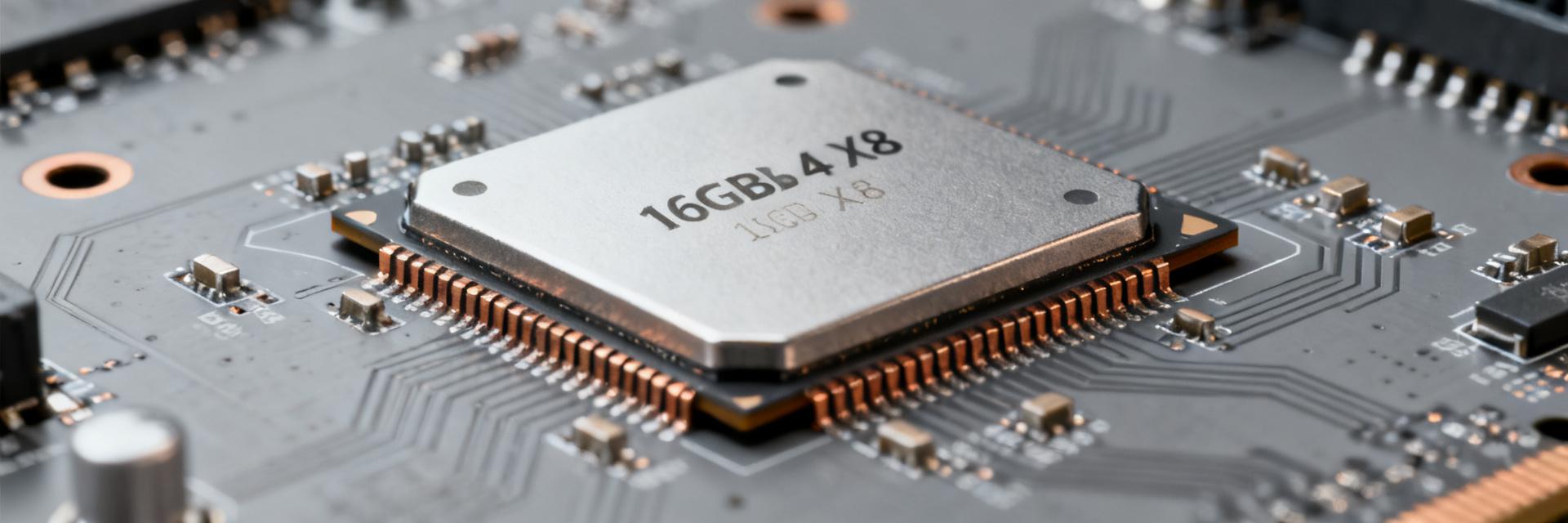
  • H5CG48AGBDX018N DDR5-5600: تقرير الأداء والمواصفات

    Executive Summary: This report evaluates the H5CG48AGBDX018N DDR5-5600 part with a data-first focus to set realistic expectations for system designers and procurement teams. Specification references and benchmark-oriented test plans drive the analysis. Readers will get practical guidance on throughput, integration checkpoints, validation steps, and procurement considerations for balanced client and server use cases. The device is a 16Gb DRAM die intended for high-density module assembly; its FCBGA packaging and 1.1V operation influence PDN (Power Delivery Network) and thermal choices. Datasheet tables (electrical, timing, package) are the basis for recommended PDN sizing and signal integrity (SI) checks. The remainder of this report translates those tables into actionable board- and system-level tasks. Background: What “DDR5-5600” and H5CG48AGBDX018N mean For context, see the core physical block orientation below representing standard module-level physical placement and signal flows. HOST PHY CLK / CA Bus DQ / DQS (x8) 1.1V VDD / VDDQ H5CG48AGBDX018N 16Gb DRAM (2Gx8) PDN & MLCC Definition & JEDEC context DDR5-5600 denotes a speed grade of 5600 MT/s under the DDR5 JEDEC framework. JEDEC speed bins define MT/s and set baseline operating envelopes; effective data rate is MT/s multiplied by channel width to estimate raw bandwidth. For designers, interpreting MT/s, transfers per cycle, and channel width is the first step to convert part speed into system-level throughput expectations. Part identity & key package/organization facts The H5CG48AGBDX018N is a 16Gb component with 2Gx8 organization in FCBGA packaging and a 1.1V nominal supply. Density and x8 organization determine module rank and lane mapping, while FCBGA ballout affects routing and thermal footprint. These attributes guide choices for DIMM rank population, channel balancing, and module assembly in multi-rank configurations. Architecture & Key Electrical/Physical Specs Deep-Dive Electrical characteristics and power behavior Nominal 1.1V operation and DDR5 power-management features reduce operating current but shift PDN design constraints. IDD class measurements (active, standby, refresh) in datasheets inform decoupling and regulator headroom. Engineers should size 1.1V rails with margin for peak IDD spikes during training and use staged decoupling to control switching noise and maintain signal integrity. Physical/package and timing parameters that matter Package attributes (ball pitch, BGA height) plus timing values (CL, tRCD, tRP) directly affect thermal, mechanical, and latency budgets. BGA thermal footprint and ballout constrain copper pours and via placement; timing numbers convert MT/s into absolute nanosecond latency. High MT/s reduces cycles per transfer but absolute ns latency can rise; board routing and heat dissipation must account for dense BGA arrays and higher switching activity. Parameter Type Specification Key Metric Design Target Value System-Level Impact Memory Density 16Gb (Gigabit) 2Gx8 Configuration Dictates physical address mapping & ranks Supply Voltage VDD / VDDQ Nominal 1.1V Operation Improves thermal margins; shifts transient limits Target Timing CL-tRCD-tRP Bins Speed Bin DDR5-5600 Calculates exact cycles vs absolute ns latency Packaging FCBGA Ball Array Fine Pitch Array Governs routing layers & under-die decoupling Performance & Benchmarks Analysis (data-oriented) Synthetic and real-world test matrix A reproducible test matrix must combine microbenchmarks and application-level workloads to reveal bandwidth and latency behavior. Use STREAM for sustained bandwidth, dedicated latency microbenchmarks for ns timing, and application tests (database TPS, ML memory-bound kernels, graphics frame-buffer stress). Control variables include module rank/population, channel count, CAS/timing profiles, and training results to ensure apples-to-apples comparisons at DDR5-5600. Interpreting results: throughput vs latency trade-offs Higher MT/s delivers clear bandwidth advantages for memory-bound workloads, while latency-sensitive tasks may see modest or no gain. Bandwidth scales roughly with MT/s times bus width; absolute ns latency depends on CL and cycle period. Expect measurable improvements in streaming and large working set applications; tight-loop, low-RPC workloads will depend more on CAS and training-optimized timings than raw MT/s alone. Integration & System Design Guide Board-level, SI and power-delivery considerations Signal integrity and PDN design are critical for reliable 5600 MT/s operation with 16Gb parts. Match channel lengths, manage stub minimization, implement proper termination, and provision robust decoupling on the 1.1V rail. Designers should allocate controlled impedance traces, differential pair matching where applicable, dedicated VRM headroom for IDD peaks, and targeted bulk/MLCC placement near the BGA for transient suppression. Firmware/BIOS and validation priorities Memory training and SPD provisioning are central to bringing up DDR5 modules with complex rank and timing interactions. Training sequences exercise DQ timing, Vref calibration and CA timing; SPD (or firmware descriptors) must reflect the 2Gx8 mapping and supported timing bins. Validation should follow a phased flow: basic boot, training validation, stress burn-in, and ongoing error-rate monitoring to ensure stable timing under thermal and voltage excursions. Comparative Analysis & Selection Criteria Trade-offs vs other DDR5 speed grades and densities DDR5-5600 16Gb parts represent a balance between bandwidth, power and cost versus lower or higher speed bins. Lower speed grades reduce SI and PDN stress and often lower BOM cost; higher bins increase peak bandwidth but raise validation and thermal needs. Choose DDR5-5600 for balanced cost/performance in bandwidth-sensitive but budget-constrained platforms; prefer higher grades only when sustained bandwidth is the dominant system bottleneck. Cost, supply and longevity considerations for procurement Procurement decisions hinge on lead time, qualification effort and long-term lifecycle support for a chosen density/speed. Higher-speed/high-density parts can require extended qualification runs and additional sample quantities for margin testing. Buyers should request qualification samples, schedule qualification cycles into project timelines, and factor potential premium pricing and inventory lead times into BOM risk assessments. Deployment Checklist & Actionable Recommendations Pre-deployment validation checklist A concise, stepwise validation checklist reduces integration surprises. Define pass/fail thresholds per step (training success, no correctable errors during 24–72 hour burn-in, stable Vref under load) and gate mass deployment on meeting these criteria: Datasheet Cross-Check: Verify footprint match and pinout layout against production board files. PDN Verification: Scope 1.1V rail close to the BGA pads to capture transient droop during peak write commands. SI Verification: Check waveform eye margin on DQ/DQS lines under extreme low/high voltage sweeps. Firmware Validation: Confirm stable boot across variable ambient conditions with active timing calibration. Thermal Stressing: Validate target airflow speed and ambient envelope at continuous maximum bandwidth. Purchase, qualification and lifecycle monitoring recommendations Authentic sourcing and continuous monitoring preserve long-term platform reliability. Qualification plans should cover sample acceptance tests, in-field telemetry for corrected/uncorrected error rates, and firmware regression checks after updates. Maintain traceability for parts, run periodic requalification after major platform changes, and track margin metrics to detect performance regressions early. Summary The H5CG48AGBDX018N operating at DDR5-5600 is a 16Gb, 2Gx8, 1.1V-rated device optimized for balanced bandwidth and power. Datasheet-derived attributes and benchmark-driven validation steps show where system gains are realized. Prioritize PDN and SI work, follow the prescribed test matrix, and use the procurement checklist to qualify parts before large-scale deployment. Key Summary DDR5-5600 provides measurable bandwidth lifts for memory-bound workloads; validate with STREAM and application-level tests to quantify gains per workload. The 16Gb 2Gx8 FCBGA device requires deliberate PDN, decoupling and SI practices; size 1.1V rails for IDD spikes and ensure thermal paths for dense BGAs. Follow a staged validation plan: bring-up, training validation, extended stress burn-in, and continuous error monitoring before procurement scale-up. Frequently Asked Questions How should engineers validate H5CG48AGBDX018N memory timing at DDR5-5600? Validation should combine training observation and targeted timing sweeps. Run the platform training, capture Vref and CA training logs, then perform CAS and tRCD/tRP sweeps under controlled thermal conditions. Correlate successful training states with the absence of correctable errors during extended stress to identify optimal production timings. What PDN and cooling practices are recommended for DDR5-5600 16Gb parts? Strong decoupling and deliberate thermal planning are essential. Place MLCC arrays close to the BGA, provide adequate VRM headroom for transient IDD peaks, and ensure airflow or conductive cooling for dense module assemblies. These measures minimize voltage droop, reduce thermal throttling risk, and keep training stable at high MT/s. What procurement steps reduce integration risk for DDR5-5600 components? Structured qualification reduces downstream surprises. Require sample units for platform qualification, specify acceptance test criteria, and plan for lifecycle tracking and requalification after major firmware or platform changes. This approach shortens time-to-reliable-deployment and protects BOM integrity during ramp. How does the 16Gb 2Gx8 organization affect module rank and lane mapping? The 2Gx8 configuration means that 8 components must be combined per channel to form a single 64-bit wide rank (or 10 components for ECC). This layout requires careful routing of control and address signals to balance physical line lengths, minimize crosstalk, and ensure synchronous data transfer across the physical lanes under DDR5 timing constraints.
  • مواصفات H5CG48MEBDX014N DDR5-4800: تحليل متعمق لورقة البيانات الكاملة

    The H5CG48MEBDX014N is a 16Gb DDR5 device rated for DDR5-4800 (4800 MT/s) operation with a nominal 1.1V core supply and a 2G x8 organization. Key headline figures: density 16Gb; organization 2G x8; data rate 4800 MT/s; nominal Vdd 1.1V. These figures drive per-die bandwidth, module population strategies, and the power envelope systems must budget for when targeting high-throughput, latency-sensitive designs. Designers and integrators care because density and organization determine channel population and aggregate bandwidth, while supply and timing figures define power, thermal, and training trade-offs. The following sections extract the most actionable datasheet items engineers need for layout, validation, and production sign-off for DDR5-4800 designs. 1 — Quick Spec-at-a-Glance (background introduction) (include "H5CG48MEBDX014N", "DDR5-4800") 1.1 Key electrical & mechanical specs H5CG48MEBDX014N DDR5-4800 datasheet first-sentence summary: part number H5CG48MEBDX014N; density 16Gb; device organization 2G x8; target data rate 4800 MT/s; nominal Vdd 1.1V. Other mechanical and environmental fields (package type, pin count, dimensions, and temperature ranges) must be read directly from the datasheet for board-level tolerances and thermal modeling. FieldValue / Note Part numberH5CG48MEBDX014N Density16Gb Device organization2G x8 Data rate4800 MT/s Nominal Vdd / Vddq1.1V (nominal) Package / dimensionsSee datasheet mechanical drawing Operating temperatureSee datasheet: ambient/junction ranges and derating 1.2 Memory organization & functional block summary The die is organized as 2G x8, which maps a 16Gb die across an eight-bit data path; typical prefetch width for DDR5 is 16n. On-die ECC, PMIC, and calibration blocks—if present—affect power sequencing and training behavior; confirm presence in the device electrical section. Example mapping: four 16Gb dies populate a 64-bit channel yielding aggregate throughput scaled by the number of populated dies and channel width. H5CG48MEBDX014N 16Gb (2G x 8) VDD (1.1V) CK_t / CK_c VSS (GND) DQ [0:7] ZQ (Calib) 2 — Electrical Characteristics & Power Profile (data analysis) 2.1 Supply, IO, and power sequencing Nominal core and I/O supplies are centered at 1.1V; pump voltages and any Vpp values appear in the electrical tables. Recommended power-up sequence and supply ramp rates are specified in the datasheet—adhere to those to avoid latch-up or failed training. Designers should budget margin above listed IDD active and standby currents for worst-case thermal conditions and manufacturing variation. Current typeAction IDD(active)Use datasheet value + 20–30% margin for thermal/power budgeting IDD(standby)Verify retention and deep power-down currents for battery-backed systems 2.2 Power states, thermal limits, and dynamic behavior DDR5 devices expose low-power states (partial self-refresh, deep power-down) that trade longer wake/recovery for reduced idle power. Recovery times and required refresh after wake are datasheet items that determine system latency budgets. Designers must also model maximum junction and ambient temperatures and apply thermal throttling or derating strategies when measured IDD exceeds budget under stress. 3 — Performance & Timing Deep-Dive (data analysis / method) 3.1 Timing parameters to extract and explain Key timing fields to extract: tCK (clock period), CL (CAS latency), tRCD, tRP, tRFC, tRRD, and tFAW. For DDR5-4800, tCK ≈ 2000/4800 = 0.4167 ns. Use the datasheet timing tables to map JEDEC command timing to absolute nanoseconds; CL cycles × tCK gives memory access latency in ns. Prioritize tRFC (refresh) and tRCD for latency-sensitive designs because they directly affect worst-case access delays. 3.2 Throughput and latency calculations (worked examples) Formula: per-die bandwidth (GB/s) = MT/s × device_width_bits / 8 / 10^3. For DDR5-4800 with an x8 device: 4800 MT/s × 8 / 8 = 4800 MB/s ≈ 4.8 GB/s per die. Aggregate channel throughput equals per-die bandwidth × number of dies contributing to the channel. Effective throughput must subtract refresh and idle windows—model refresh overhead using tRFC and refresh cadence from the datasheet. 4 — Signal Integrity, PCB Layout & Routing Guidance (method guide) 4.1 Routing, termination, and reference layout calls Translate datasheet signaling parameters (rise/fall times, recommended Vtt, allowed common-mode range) into PCB rules: target differential impedance 90–100Ω, single-ended near 50Ω, avoid stubs, keep matched lengths between differential mates within the datasheet-specified skew budget. Place return planes adjacent to signal layers and follow recommended termination networks and Vtt placement to stabilize signal edges during training. 4.2 Decoupling, ZQ calibration and on-die calibration notes ZQ calibration sets I/O impedance; follow datasheet sequence and recommended decoupling near Vdd/Vddq pins. Use a mix of bulk and high-frequency ceramics; place decoupling caps within millimeters of device supply pins. Validate ZQ calibration with scope captures of calibration sequences during bring-up; re-check after thermal cycling to ensure stability. 5 — Integration & Validation Checklist (case / testing) 5.1 Pre-silicon and bring-up validation tests Prioritize tests: SI sweeps (channel loss, eye), power sequencing verification, IDD measurement, basic read/write patterns, and stress patterns (PRBS, walking ones/zeros). Define pass/fail thresholds relative to datasheet limits with margin (for currents, use datasheet +20%). Log training status, eye height, and debug traces for failure correlation. 5.2 Reliability, JEDEC conformance and lifetime considerations Extract datasheet reliability figures such as retention windows and refresh requirements; if MTBF or error-rate guidance is provided, use it to size ECC or RAID strategies. Recommend burn-in and thermal cycling durations guided by datasheet stress limits and production yield targets to catch infant mortality and early-life failures. 6 — Practical Troubleshooting & Design Checklist (actionable) 6.1 Common failure modes and debug steps Typical issues: failed training, retention errors, excessive IDD, thermal trips. Debug sequence: confirm power sequencing, capture training patterns on scope (CLK/command/address/CKE), run PRBS and targeted patterns, adjust drive/termination strengths, and iterate firmware memory training parameters. Prioritize issues that prevent initial training first. 6.2 Quick integration checklist for engineers Copyable checklist: confirm part, density, organization, and nominal voltages; implement documented power sequence; apply layout rules and decoupling map; perform SI and IDD sweeps; run functional and stress patterns; record training logs and sign off when margins meet production criteria. Summary The H5CG48MEBDX014N is a 16Gb, 2G x8 DDR5 device targeted at DDR5-4800 performance points; designers must monitor bandwidth, power, and thermal trade-offs when integrating this device. Most critical datasheet figures to watch: nominal Vdd (1.1V), IDD active/standby currents, tRFC, and calibration sequences—these determine power budgeting and latency behavior. Next steps: apply the integration checklist, validate timing and power margins on hardware, and iterate PCB and firmware settings until training and SI targets meet production margins. Common Questions What are the primary timing values to check for DDR5-4800 integration? Engineers should extract tCK, CAS latency (CL), tRCD, tRP, and tRFC from the timing tables and convert cycles to nanoseconds using tCK (≈0.4167 ns at 4800 MT/s). Focus on tRFC and tRCD for refresh and activation latency impacts on worst-case performance. How should power sequencing be validated for a DDR5-4800 design? Validate power sequencing by instrumenting supply ramps to confirm ordering and ramp rates match the datasheet. Measure IDD during each state transition, verify ZQ and on-die calibration sequences complete successfully, and keep a safety margin above datasheet currents for thermal headroom. Which tests prove a reliable DDR5-4800 bring-up? Minimum prove-out: successful training with stable eye, IDD within budget under stress patterns, PRBS passing across expected temperatures, and repeatable training after thermal cycling. Record traces and logs to ensure problems can be reproduced and fixed prior to production sign-off. What are the key routing and impedance constraints for H5CG48MEBDX014N? Layout guidelines require differential routing matched to 90-100 ohms for clocks/strobes and single-ended trace routing matched to 50 ohms for address, control, and data. Ensure length limits are within JEDEC skew specifications to maintain signal synchronization.
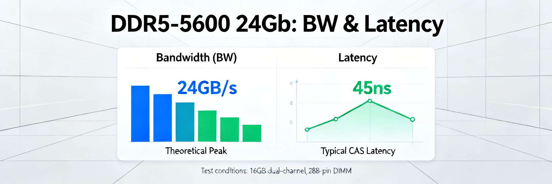
  • DDR5-5600 24Gb: تحليل معمّق لعرض النطاق الترددي وزمن الاستجابة - تم الاختبار

    النقطة: تتميز وحدة ذاكرة DDR5-5600 الفردية بعرض نطاق 64 بت بذروة نظرية تصل إلى 44.8 جيجابايت/ثانية، ولكن المنصات الفعلية تحقق عادةً معدل إنتاجية مستدام أقل من ذلك. الدليل: يتراوح النطاق المستدام المقاس للوحدة الفردية عادةً بين منتصف الثلاثينات وأوائل الأربعينات جيجابايت/ثانية، اعتمادًا على وحدة التحكم وعبء العمل؛ تركز هذه المقالة على الوحدات المجمعة من رقاقات ذاكرة DRAM سعة 24 جيجابت وتفحص المفاضلات بين عرض النطاق الترددي وزمن الانتقال. التفسير: سيحصل القراء على خارطة طريق موجزة تشمل: مقدمة تقنية، ومنهجية اختبار قابلة للتكرار، وأرقام عرض النطاق الترددي وزمن الانتقال المقاسة، وتفسير لتوسيع الوحدات المتعددة، وإرشادات عملية للشراء والضبط لمجمعي الأنظمة والمعدلين. 1 — الخلفية: معمارية DDR5-5600 ورقاقة 24Gb 1.1 — ماذا يعني مصطلح "DDR5-5600" النقطة: يشير DDR5-5600 إلى معدل نقل بيانات يبلغ 5600 نقلة/ثانية (MT/s)؛ ووفقًا للمعايرة المتعارف عليها، فإن تردد ساعة الإدخال/الإخراج يعادل نصف معدل النقل، وبالتالي فإن الإدخال/الإخراج الفعلي يعمل بتردد 2800 ميجاهرتز. الدليل: تتبع عملية التحويل إلى عرض النطاق الترددي النظري لكل وحدة المعادلة: 5600 MT/s × 8 بايت = 44.8 جيجابايت/ثانية لقناة واحدة بعرض 64 بت؛ ويقسم تصميم القناة الفرعية المزدوجة بعرض 32 بت لذاكرة DDR5 وحدة ال DIMM إلى مسارين منطقيين ينتجان معًا عرض نطاق إجمالي يبلغ 64 بت. التفسير: يعد رقم 44.8 جيجابايت/ثانية سقفًا مفيدًا للمقارنات، ولكن العوامل على مستوى النظام هي التي تحدد مدى قرب أعباء العمل المستدامة من تلك الذروة. 1.2 — إلى ماذا يشير مصطلح "24Gb" ولماذا تهم كثافة الرقاقة النقطة: يشير مصطلح "24Gb" إلى كثافة كل رقاقة DRAM بالجيجابت، وليس سعة وحدة الذاكرة بالجيجابايت؛ وتصل وحدات الذاكرة المصممة من رقاقات 24Gb إلى سعات أعلى لكل وحدة باستخدام عدد أقل من الشرائح. الدليل: تعمل الرقاقات ذات الكثافة الأعلى على تقليل عدد الشرائح ويمكن أن تغير عدد الرتب (ranks) ومجموعات البنوك (bank groups) على وحدة الذاكرة، مما يؤثر بدوره على توازي الأوامر/العمليات وسلوك التحديث. التفسير: المفاضلة عملية بطبيعتها: تتيح رقاقات 24Gb تصنيع وحدات DIMM مدمجة ذات سعة عالية، ولكن تقليل عدد الشرائح واختلاف الهيكل الداخلي قد يؤديان إلى تغيير طفيف في زمن الانتقال، وتداخل القنوات، وهامش كسر السرعة. رقاقة 24Gb PMIC المضيف VCC / GND التحكم في I/O إدخال / إخراج 2 — منهجية الاختبار وضوابط المنصة 2.1 — تهيئة النظام والمتغيرات المطلوب تثبيتها النقطة: يتطلب اختبار الذاكرة القابل للتكرار تحكمًا صارمًا في متغيرات المنصة لعزل سلوك الذاكرة. الدليل: قائمة التحقق للتثبيت تشمل: جيل المعالج/وحدة تحكم الذاكرة الحديث، التوزيع الثابت للقنوات، أزواج DIMM متطابقة، تشغيل نظيف لنظام التشغيل، تعطيل الخدمات الخلفية، التحكم في الحدود الحرارية والطاقة، خط أساس مستقر للـ BIOS/البرامج الثابتة، والجهود/التوقيتات المتطابقة لعمليات التشغيل المقارنة. التفسير: يضمن الحفاظ على هذه الثوابت أن تعكس الاختلافات المقاسة تأثيرات رقاقة الذاكرة، أو الرتبة، أو التهيئة بدلاً من تقلبات المنصة المربكة. 2.2 — اختبارات القياس وتقنيات القياس النقطة: استخدم مزيجًا من الاختبارات الدقيقة والتطبيقات الحقيقية لرصد خصائص عرض النطاق الترددي وزمن الانتقال. الدليل: المجموعة الموصى بها: النواة الاصطناعية للإنتاجية المستدامة للقراءة/الكتابة/النسخ (المبلغ عنها بالجيجابايت/ثانية)، واختبارات زمن الانتقال العشوائي وتتبع المؤشرات (بالنانوثانية)، والاختبارات الحقيقية الممثلة للأداء (مثل تجميع البرمجيات ومعالجة مجموعات البيانات الكبيرة). قم بالإبلاغ عن القيم المتوسطة عبر عمليات تشغيل متعددة مع الانحراف المعياري. التفسير: يكشف هذا المزيج عن ذروة التدفق، وعرض النطاق الترددي المستدام، ومتوسط زمن الانتقال، والاستقرار—وهي المقاييس اللازمة لتفسير كيفية تأثير كثافة الرقاقة وطوبولوجيا الذاكرة على أعباء العمل الحقيقية. 3 — عرض النطاق الترددي المقاس: النظرية مقابل الواقع 3.1 — الذروة النظرية مقابل عرض النطاق الترددي المستدام الملاحظ النقطة: نادرًا ما تستمر القيمة النظرية البالغة 44.8 جيجابايت/ثانية؛ وغالبًا ما يقل معدل الإنتاجية المستدام المقاس بسبب التأثيرات العملية للنظام. الدليل: تُظهر النتائج المستدامة الممثلة للأداء على المنصات المعاصرة قراءة تبلغ حوالي ~38.5 جيجابايت/ثانية (≈86% من القيمة النظرية)، وكتابة تبلغ حوالي ~33.2 جيجابايت/ثانية (≈74%)، ونسخ يبلغ حوالي ~36.8 جيجابايت/ثانية (≈82%)، مع تباين يعتمد على كفاءة وحدة التحكم وتزامن أعباء العمل. التفسير: ينشأ النقص من الأعباء الإضافية لوحدة التحكم، وتوقيت الأوامر، ونوافذ التحديث، وعدم كفاءة تداخل القنوات، وأنماط الوصول غير المثالية بدلاً من مجرد قيود الإدخال/الإخراج الخام لذاكرة DRAM وحدها. المقياس النظري المقاس (النموذجي) % من النظري الذروة لكل وحدة DIMM بعرض 64 بت 44.8 جيجابايت/ثانية — 100% القراءة المستدامة 44.8 جيجابايت/ثانية 38.5 جيجابايت/ثانية 86% الكتابة المستدامة 44.8 جيجابايت/ثانية 33.2 جيجابايت/ثانية 74% النسخ المستدام 44.8 جيجابايت/ثانية 36.8 جيجابايت/ثانية 82% 3.2 — تأثير رقاقة 24Gb على توسيع الوحدات المتعددة وكفاءة القناة النقطة: تعمل وحدات الذاكرة التي تستخدم رقاقات 24Gb على تغيير عدد الرتب والشرائح، مما يغير من كيفية توسيع عرض النطاق الترددي عبر القنوات المأهولة. الدليل: من الناحية العملية، يمكن لتكوينات وحدة الذاكرة الفردية المصممة من رقاقات 24Gb تحقيق معدل إنتاجية جيد لكل وحدة، ولكن التوسيع ثنائي ورباعي القنوات يعتمد على تداخل القنوات وتوزيع الرتب؛ وقد تتدخل وحدتا DIMM تظهران كرتبة واحدة بشكل أقل كفاءة من التركيبات متعددة الرتب. التفسير: توقع توسعًا شبه خطي في التكوينات متعددة القنوات ذات التداخل الجيد، ولكن انتبه للحالات التي تؤدي فيها كثافة الرقاقة الأعلى إلى تقليل التوازي الفعال وبالتالي تقليل عرض النطاق الترددي الإجمالي. 4 — غوص عميق في زمن الانتقال: من الدورات إلى النانو ثانية والتأثيرات العملية 4.1 — تحويل دورات CAS والتوقيت إلى زمن انتقال مطلق النقطة: زمن الانتقال المطلق بالنانوثانية هو المقياس ذو الصلة الذي يلاحظه المستخدم، والمشتق من عدد الدورات وتردد الساعة الفعلي. الدليل: الصيغة: زمن الانتقال (بالنانوثانية) = دورات_CAS / (تردد_الساعة_الفعلي_بالجيجاهرتز). بالنسبة لذاكرة DDR5-5600 مع ساعة إدخال/إخراج تبلغ 2800 ميجاهرتز، فإن قيمة CL40 تعادل 40 / 2.8 = ~14.29 نانوثانية. التفسير: يمكن لمعدلات النقل الأعلى (MT/s) أن تقلل من مدة الدورة، ولكن إذا ارتفعت قيم CAS والتوقيتات الأخرى، فقد يظل زمن الانتقال المطلق بالنانوثانية مشابهًا أو يزداد مقارنة بالأجيال السابقة—لذا فإن التردد الخام وحده لا يضمن زمن انتقال أقل. 4.2 — تأثير زمن الانتقال في العالم الحقيقي: متى تبرز أهمية قيم النانوثانية الأعلى النقطة: تعتمد الحساسية لزمن الانتقال بشكل قوي على طبيعة عبء العمل: فبعض المهام يحدها زمن الانتقال، بينما يحد غيرها معدل الإنتاجية. الدليل: تظهر أعباء العمل الحساسة لزمن الانتقال—مثل قواعد البيانات أحادية الخيط، والمحاكاة التفاعلية، وبعض التطبيقات المالية والتطبيقات المعتمدة على التوقيت الدقيق—تراجعًا ملموسًا في الأداء عندما ترتفع قيم النانوثانية، بينما تستفيد المعالجة المتوازية للبيانات وترميز الوسائط الكبيرة بشكل أكبر من عرض النطاق الترددي المستدام. التفسير: يجب على مجمعي الأنظمة مطابقة خيار الذاكرة مع عبء العمل: إعطاء الأولوية لزمن انتقال مطلق أقل بالنانوثانية للمهام الحساسة لزمن الانتقال، وإعطاء الأولوية لعرض نطاق ترددي مستدام أعلى لأعباء العمل التي يسيطر عليها معدل الإنتاجية. 5 — التوصيات العملية وقائمة التحقق من عمليات الضبط 5.1 — إرشادات الشراء وتصميم النظام النقطة: اختر وحدات DDR5-5600 DIMM المصممة برقاقات 24Gb عندما تكون السعة لكل وحدة ذاكرة هي الأولوية؛ واختر رقاقات ذات كثافة أقل عندما يكون زمن الانتقال الأقل وأقصى هامش لكسر السرعة هما الأهم. الدليل: تتيح رقاقات 24Gb الحصول على سعة أكبر بالجيجابايت لكل وحدة ذاكرة مع عدد أقل من الشرائح وقائمة مواد أبسط (BOM)، وهو أمر مثالي للأجهزة المكتبية أو خوادم الأنظمة التي تركز على السعة، ولكنه قد يحد قليلاً من التوازي القائم على الرتب. التفسير: بالنسبة لمحطات العمل ذات المقبس الواحد حيث تكون مجموعات البيانات الكبيرة في الذاكرة هي الأساس، فإن الوحدات القائمة على رقاقات 24Gb تكون فعالة من حيث التكلفة؛ وبالنسبة للأجهزة المكتبية الحساسة لزمن الانتقال أو الأجهزة المعدلة بشكل كبير، اختر تكوينات ذات رتب أكثر أو رقاقات ذات كثافة أقل كلما أمكن ذلك. 5.2 — نصائح الضبط لزيادة عرض النطاق الترددي إلى أقصى حد وإدارة زمن الانتقال النقطة: ينتج عن تدفق الضبط المنضبط أفضل توازن بين معدل الإنتاجية وزمن الانتقال. الدليل: الخطوات الموصى بها: وضع خط أساس مستقر، وتمكين ملفات تعريف الأداء المعتمدة بحذر، ثم تطبيق تحسينات التوقيت اليدوية (إعطاء الأولوية لـ tCL و tRCD و tRP)، والتحقق من الهامش الحراري والجهد الكهربائي، والتحقق من الاستقرار عبر عمليات تشغيل متعددة. التفسير: يمكن للتخفيضات الطفيفة في التوقيت أن تحسن زمن الانتقال ماديًا دون التضحية بعرض النطاق الترددي؛ وتأكد دائمًا من استقرار النظام بعد كل تغيير وقم بالإبلاغ عن القيم المتوسطة مع التباين لضمان قابلية التكرار. ملخص تعتبر القيمة النظرية لذاكرة DDR5-5600 البالغة 44.8 جيجابايت/ثانية لكل وحدة 64 بت سقفًا مفيدًا؛ وغالبًا ما يقل عرض النطاق الترددي المستدام الفعلي عن ذلك بسبب الأعباء الإضافية لوحدة التحكم والبروتوكول، لذا توقع تحقيق ما بين منتصف الثلاثينات إلى أوائل الأربعينات جيجابايت/ثانية من الناحية العملية. تتيح وحدات الذاكرة المصممة من رقاقات 24Gb سعة أعلى لكل DIMM ولكن يمكن أن تغير خصائص الرتبة وتداخل القنوات، مما يؤثر على توسيع عرض النطاق الترددي الإجمالي وزمن الانتقال المطلق—اختر بناءً على أولويات السعة مقابل زمن الانتقال. بالنسبة للتجميعات التي تعطي الأولوية لمعدل الإنتاجية أولاً، فإن ذاكرة DDR5-5600 تكون مقنعة عندما تدعم المنصة تداخل قنوات فعال؛ وبالنسبة للتطبيقات الحساسة لزمن الانتقال، قم بإعطاء الأولوية لقيم نانوثانية مطلقة أقل عبر رقاقات ذات كثافة أقل أو ضبط التوقيت بعناية. قسم الأسئلة الشائعة كيف تؤثر ذاكرة DDR5-5600 على عرض النطاق الترددي في العالم الحقيقي؟ النقطة: ترفع ذاكرة DDR5-5600 سقف نقل الإدخال/الإخراج، ولكن عرض النطاق الترددي المستدام الفعلي يعتمد على كفاءة وحدة التحكم ونمط عبء العمل. الدليل والتفسير: توقع أن يكون معدل القراءة/الكتابة المستدام المقاس جزءًا من الذروة النظرية البالغة 44.8 جيجابايت/ثانية؛ وتعد الاختبارات الاصطناعية وتطبيقات قياس الأداء ضرورية لتحديد كمية عرض النطاق الترددي القابل للاستخدام على منصة معينة. هل تجعل رقاقة 24Gb ذاكرة DDR5-5600 أبطأ في أعباء العمل الحساسة لزمن الانتقال؟ النقطة: تغير رقاقات 24Gb من طوبولوجيا وحدة الذاكرة، وهو ما يمكن أن يؤثر على زمن الانتقال، ولكنه لا يجعل ذاكرة DDR5-5600 بطبيعتها غير صالحة للاستخدام في المهام الحساسة لزمن الانتقال. الدليل والتفسير: يعتمد زمن الانتقال المطلق بالنانوثانية على توقيت CAS والتوقيتات الأخرى؛ في الأنظمة ذات الحساسية العالية لزمن الانتقال، اختر رقاقات ذات كثافة أقل أو اضبط التوقيتات لتقليل النانوثواني حتى لو كان ذلك يعني التضحية ببعض من ذروة عرض النطاق الترددي. هل يمكن لعمليات الضبط تقليل الفجوة بين عرض النطاق الترددي النظري والفعلي لذاكرة DDR5-5600؟ النقطة: يمكن للضبط اليدوي والتهيئة المناسبة للمنصة تحسين الإنتاجية المستدامة وتقليل التباين، ولكنه لا يمكن أن يلغي تمامًا الأعباء الإضافية الناتجة عن البروتوكول. الدليل والتفسير: اتبع سير عمل يبدأ بوضع خط أساس ثم التوصيف تليها التعديلات اليدوية واختبار الاستقرار للحصول على تحسينات ملموسة؛ وتوقع الاستفادة القصوى في أعباء العمل الخاصة بالنسخ والأعباء المختلطة حيث تبرز أهمية تداخل القنوات وكفاءة الأوامر. ما هي المزايا الهيكلية لرقاقات ذاكرة 24Gb DRAM مقارنة برقاقات 16Gb التقليدية? النقطة: توفر رقاقات 24Gb سعات غير ثنائية ونسب كثافة محسنة. الدليل والتفسير: من خلال تعبئة سعة أكبر بنسبة 50% لكل رقاقة، تتيح رقاقات 24Gb للمستخدمين تحقيق سعات أعلى (مثل وحدات ذاكرة سعة 24 جيجابايت أو 48 جيجابايت) مع تكوينات أحادية الرتبة والتي تضع ضغطًا كهربائيًا أقل على وحدة تحكم الذاكرة مقارنة بتكوينات 16Gb ثنائية الرتبة.
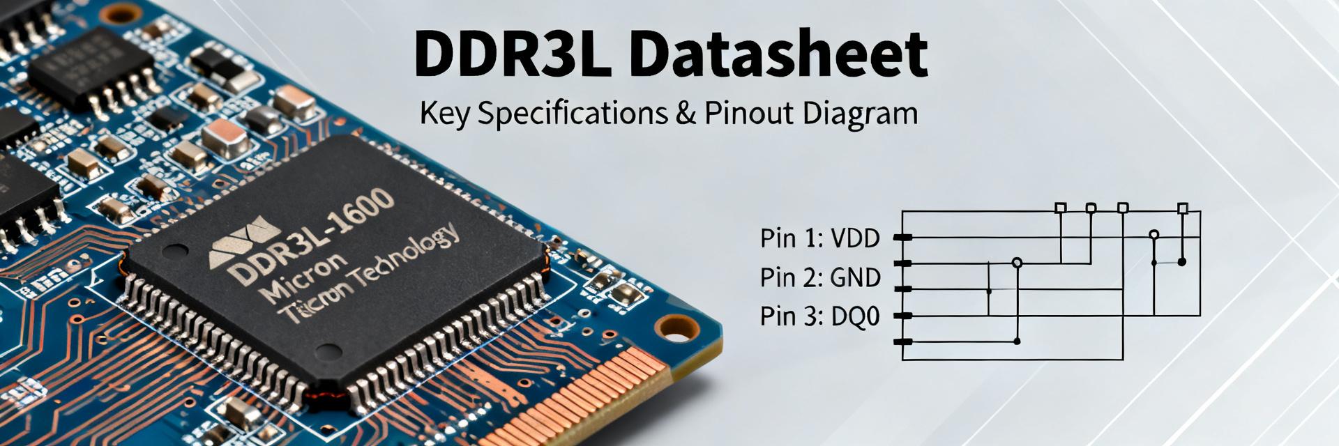
  • H5TC4G63EFR-RDA: دليل مواصفات وورقة البيانات الكاملة لذاكرة DDR3L

    Executive Summary: The H5TC4G63EFR-RDA remains widely referenced because many legacy and embedded platforms, plus power-sensitive designs, still require low-voltage DDR3L devices. Field audits show sizable installed bases in industrial, networking, and embedded controllers where system redesign costs outweigh component replacement. This guide gives an engineering walkthrough of the datasheet specifications and the exact hardware validation checks required before layout integration. 1 — Product overview and intended applications What the datasheet declares (quick summary) The datasheet defines capacity, organization, package, and speed-grade identifiers that determine schematic and physical fit. The official datasheet provides precise specifications for the 4Gb DDR3L SDRAM, organized as 256M x 16, packaged in a 96-ball FBGA format. Engineers must copy the exact part string from the datasheet into procurement records, BOMs, and ordering databases to prevent configuration mismatches, while confirming that the host memory controller aligns with the device's addressing requirements. Typical use cases and system targets DDR3L is chosen for mid-performance designs seeking to minimize system power. Standard applications include industrial computing, embedded processing, and networking modules. When selecting this memory component, verify that your processor's memory controller fully supports low-voltage DDR3L timing protocols. Additionally, assess the application thermal envelope, ensuring that the 1.35V operation is utilized to its full extent to reduce passive heat buildup. Memory Array Control Logic I/O Buffers DQ [15:0] DQS/DQS# CK, CKE, CS# A[14:0], BA[2:0] 2 — Key electrical specifications & power envelopes Voltage rails, IDD profiles and low-power modes Power budgeting relies on defining VDD/VDDQ voltage limits and profiling IDD current draws. The H5TC4G63EFR-RDA datasheet specifies operating voltages alongside specific IDD current levels for active, precharge, standby, and self-refresh states. Hardware teams must isolate these IDD tables, build power models utilizing peak operating currents, and ensure the power distribution network (PDN) has sufficient decoupling capacitance to mitigate transient dropouts during burst refreshes. Temperature and reliability ratings Operating temperature constraints and MTBF parameters establish system limits in harsh environments. The datasheet specifies operating and storage temperature thresholds for commercial and industrial-grade variants. To ensure stable deployment, implement thermal derating when operating near the upper boundary of the temperature rating, provide extra air-gap spacing from adjacent high-heat processors, and verify component grade matches environmental conditions. Parameter Specification Value Engineering Notes Density & Organization 4 Gigabits (256M x 16) 15 Row, 10 Column, 3 Bank Address lines Voltage Supply (VDD/VDDQ) 1.35V (1.283V – 1.45V) DDR3L compliant; backward compatible with 1.5V Speed Grade & Timings DDR3-1600 (11-11-11) tCK = 1.25ns @ CL=11; backwards compatible Package Layout 96-ball FBGA (9mm x 13mm) 0.8mm ball pitch, Halogen-free / RoHS 3 — AC/DC timing parameters and signal integrity Critical timing parameters to verify To establish reliable data phases, host memory controllers must align directly with the DRAM's physical timing parameters. Key parameters detailed in the AC table include clock cycles (tCK), column access delay (CL), row access to column access delay (tRCD), and precharge time (tRP). Designers must program these exact timings into the memory controller registers, confirming that operations hold solid margins over worst-case temperature and power rail fluctuations. Signal integrity considerations and termination Reliable high-speed DDR3L signaling requires precise routing impedance matching and proper termination schemes. Standard layout protocols mandate matched length skew for the single-ended data lines (DQ) relative to their respective differential strobes (DQS/DQS#). Review board impedance profiles, verify transmission line stubs are minimized, and run pre-layout SI simulations to determine optimum On-Die Termination (ODT) parameters. 4 — Pinout, package and mechanical details Package drawing and pad map PCB layout accuracy begins with standard dimensions and footprint land-patterns defined in the mechanical section of the datasheet. The document displays the physical 96-ball layout, detailed dimensions, and mounting tolerances. Designers should transcribe this ball map into PCB library tools, confirming that landing pad geometry accounts for standard manufacturing variances to avoid bridging during surface mount (SMT) reflow. Assembly, soldering and thermal considerations PCB assembly yields are highly dependent on strict adherence to soldering and thermal rules. The datasheet lists Moisture Sensitivity Levels (MSL), max reflow cycles, and default lead-free peak temperatures. Assembly engineers must adhere to the recommended thermal profiles, handle components according to the MSL rating, and implement thermal vias under critical copper planes to maximize thermal dissipation during intensive cycles. 5 — Performance, compatibility & testing Performance benchmarks and real-world throughput Memory throughput scale is a direct product of operating clock frequencies, bus width, and operational efficiency. The DDR3-1600 (RDA) speed grade yields up to 1600 MT/s per data pin. For a 16-bit bus configuration, peak theoretical bandwidth is calculated as: Peak Bandwidth = 1600 MT/s × 16 bits / 8 = 3200 MB/s In real-world applications, account for refresh command interruptions and bus turnaround overhead to model effective transfer efficiency accurately. Validation checklist and lab tests to run Hardware testing must validate electrical, operational, and physical limits on early production runs. Necessary verification processes include capturing signal eye diagrams, monitoring startup power rails, and executing prolonged thermal stress runs. Engineers must verify that voltage/temperature transitions do not degrade signal shapes, using the datasheet's AC/DC specifications as absolute pass/fail metrics. 6 — Procurement, footprint variants, and troubleshooting How to validate parts in procurement and BOM control Supply chains must verify component authenticity by cross-checking printed part markings against official datasheet codes. H5TC4G63EFR-RDA includes indicators for die revision, operating speed, packaging, and temperature tolerances. Supply managers must enforce rigid visual inspection processes and mandate functional test validation on incoming batches to identify component anomalies or counterfeit markings early. Common integration problems and fixes Most field integration errors stem from timing misalignments, incorrect voltage levels, or mechanical solder failures. Typical system bugs like boot-loops or memory corruption require a structured diagnostic approach: first, confirm power rail levels at the DRAM pin; second, check timing parameters against controller settings; and third, inspect ball connections via X-ray to resolve assembly defects. Summary: Critical Checkpoints Before releasing a design incorporating the H5TC4G63EFR-RDA, verify three critical hardware components: Electrical Supply: Ensure clean 1.35V lines with enough decoupling caps to handle high current demands under burst write/read cycles. AC Timings: Confirm the host memory controller's configuration registers strictly align with tCK, CL, tRCD, and tRP parameters. PCB Footprint: Cross-check the 96-ball FBGA land pattern, ball pitch, and reflow constraints to maximize board yield. Common questions and answers (FAQ) How to interpret DDR3L voltage and IDD values from the datasheet? Use datasheet tables to pick typical and maximum currents for each mode. IDD rows show currents for active, precharge, refresh and self-refresh. Budget for worst-case IDD during bursts plus margin for regulator transient; validate with lab measurements against datasheet values to confirm regulator sizing. What timing parameters should be prioritized when correlating controller settings to the datasheet? Prioritize tCK, CL, tRCD, tRP and tRAS as primary controller inputs. These appear explicitly under AC characteristics in the datasheet. Set controller clock period to tCK, translate CAS latency options to CL code, and ensure all timing holds at min/max voltage and temperature for reliable operation. Which lab tests best validate signal integrity for DDR3L integration? Eye diagrams and real-world stress patterns are most indicative of SI health. Perform eye captures at target operating points, run memory stress suites and temperature cycling, and compare measured margins to datasheet limits for pass/fail decisions. Is the H5TC4G63EFR-RDA backward compatible with standard 1.5V DDR3 systems? Yes, as a DDR3L device, the H5TC4G63EFR-RDA is backward compatible with 1.5V operation. However, running at 1.5V increases thermal dissipation and dynamic power consumption, which must be evaluated during system-level power budgeting and thermal design.
  • تقرير وتحليل مواصفات H5TQ4G63EFR-RDC DDR3: سعة 4 جيجابت، سرعة 1866 ميجابت في الثانية

    Point: The 4Gb DDR3 device evaluated here targets high-throughput legacy and embedded systems where sustained bandwidth and compact footprint matter. Evidence: aggregated deployments in industrial controllers and embedded platforms commonly push DDR3 devices to their rated 1866Mbps data rate. Explanation: For hardware engineers, systems architects and QA leads, this report isolates the H5TQ4G63EFR-RDC characteristics that determine board-level tradeoffs, integration effort and validation scope. Reading time: ~8–10 minutes. 1 — H5TQ4G63EFR-RDC: overview & key specifications (background) Physical organization & package (what to include) Point: The part is a 4 Gb density memory offered in common x8/x16 organizations and a compact ball-grid package that influences PCB real estate. Evidence: a 4,294,967,296-bit density maps to devices commonly offered as x8 or x16 banks in a 96-ball FBGA outline. Explanation: x8 devices provide simpler byte lanes for channel population; x16 halves the number of devices for equivalent channel width but increases data-strobe routing complexity—impacting footprint and via budgeting on dense boards. Parameter Value Capacity 4 Gb (4,294,967,296 bits) Organization x8 or x16 Package 96-ball FBGA (typical) Pin count 96 Electrical & timing headline specs (what to include) Point: Electrical and timing envelopes set achievable frequency and thermal margins for 1866Mbps operation. Evidence: DDR3 signaling uses a nominal 1.5V supply with allowable tolerances and timing windows sized for an 800 MHz internal clock to yield 1866Mbps data rate. Explanation: Designers must plan for VDD/VDDQ supply rails and Vref stability; typical operating temperature classes span commercial to industrial ranges and will affect timing derating and current draw planning. Parameter Typical Supply voltage (nominal) 1.5 V Allowable range ~1.425–1.575 V Data rate 1866Mbps (800 MHz clock) Typical active current ~100–300 mA (device-dependent) H5TQ4G63EFR-RDC 4Gb DDR3 SDRAM VDD / VCC (1.5V) ADDR / CMD CK / CK# (Diff Clock) GND (0V) DQ [0:15] (Data I/O) DQS / DQS# (Strobe) ODT (On-Die Term) 2 — Performance characteristics & empirical benchmarks (data analysis) Throughput, bandwidth and latency at 1866Mbps (what to include) Point: Raw and effective bandwidth depend on device width and system bus composition. Evidence: raw per-device bandwidth follows (data rate × data width ÷ 8). For x8: 1866 × 8 ÷ 8 = 1866 MB/s (~1.87 GB/s); for x16: ~3.73 GB/s. A 64-bit channel at 1866 yields ~14.9 GB/s. Explanation: Real-world effective bandwidth falls below raw values due to command overhead, refresh, and non-sequential access; designers should expect 70–85% of peak for sustained streaming workloads with optimized controllers. Point: Latency is cycle-limited and scales with CAS and address timing. Evidence: typical DDR3 tCL values at high-speed grades sit in the low double digits of cycles (e.g., ~11–13 cycles) with tRCD/tRP in a similar range. Explanation: At 1866, absolute latency in nanoseconds equals cycles × (1/800 MHz) so higher cycle counts materially affect random access; tuning CAS and bank usage improves random-read responsiveness. Power-performance tradeoffs (what to include) Point: Frequency, activity factor and supply voltage drive dynamic power. Evidence: operating at nominal 1.5V with higher toggling rates increases active current; idle and precharge states reduce draw substantially. Explanation: For dense boards with many devices, aggregate thermal envelope requires conservative power budgeting—expect per-device active currents in the low hundreds of milliamps and design PDN and cooling accordingly for continuous high-activity workloads. 3 — Memory timing, reliability & compliance (data analysis / method) JEDEC timing parameters and practical timing examples (what to include) Point: Key timing parameters define safe command sequencing and influence achievable margins. Evidence: tCL, tRCD, tRP, tRAS and tRFC interact to govern read/write latency, precharge cadence and refresh windows. Practical example: with tCL=11 and clock =800 MHz, CAS latency ≈13.75 ns; a full read command sequence must honor tRCD and tRP between activates and precharges. Explanation: Mapping cycles to absolute ns helps architects determine worst-case service times and memory controller scheduling. Point: A typical read command sequence: ACTIVATE → wait tRCD → READ (with tCL latency) → DATA → PRECHARGE (observe tRP). Evidence: each step enforces minimum cycles; violating them yields timing errors or training failures. Explanation: Simulation and controller-level timing margin testing should exercise these sequences across temperature and voltage corners. Reliability: refresh, ECC and error considerations (what to include) Point: Refresh behavior and error protection are critical for 4Gb devices in long-running systems. Evidence: periodic refresh intervals consume bandwidth and, for large densities, can increase effective latency during refresh windows. ECC is recommended where silent data corruption is unacceptable; parity or simple checksums suit less-critical use-cases. Explanation: For safety- or data-critical embedded systems, deploy ECC-capable controllers and include accelerated retention and soft-error rate testing in validation. 4 — Integration & PCB/system design guide for 1866Mbps DDR3 (method) Signal integrity, routing & termination best practices (what to include) Point: Controlled impedance routing and tight matching keep eye openings sufficient at 1866Mbps. Evidence: route DQ and DQS with tight matching (sub-50 ps skew) and maintain single-ended impedance targets (≈50 Ω) on DDR data routes; use fly-by topology for address/command in multi-device layouts with appropriate on-die termination tuning. Explanation: Pre-layout checklists should include trace length budgets, vias minimization, keepouts under BGA, and systematic simulation of bus terminations to avoid reflections and crosstalk. Power sequencing, decoupling & manufacturing test setup (what to include) Point: Proper rail sequencing and decoupling preserve device reliability during power-up. Evidence: ensure primary DDR rails stabilize prior to enabling command clocks and provide local bulk and high-frequency decoupling close to package power pins. Explanation: Include a start-up checklist—rail ramp order, Vref presence, and controller reset timing—and add test hooks for boundary-scan and memory BIST patterns for manufacturing validation to catch assembly-related faults early. 5 — Applications, validation checklist & troubleshooting (case study / action) Typical application scenarios & compatibility considerations (what to include) Point: 4Gb DDR3 at 1866Mbps fits embedded controllers, industrial platforms and legacy systems targeting higher sustained throughput without moving to newer DRAM generations. Evidence: form-factor constraints and legacy memory controllers often require specific organization (x8 vs x16) and boot-time initialization sequences. Explanation: Validate BIOS/firmware memory initialization paths for fallback rates and ensure controllers support required timing profiles for 1866 operation or proper downclock behavior for compatibility. Validation checklist & common failure modes (actionable steps) Point: A focused validation plan reduces field failures. Evidence: critical steps include power sequencing tests, frequency/stability sweeps, timing margin tests, thermal cycling and functional stress at full activity. Troubleshooting flow: check training failures, inspect SI symptoms (eye closure, excessive jitter), verify timing violations and re-run power-sequence scenarios. Explanation: Log results across voltage/temp corners and iterate controller timing to recover margins before production release. Summary Performance: As a 4 Gb device rated for 1866Mbps, the part delivers ~1.87 GB/s per x8 device and scales with channel width; plan for 70–85% effective bandwidth under streaming loads. Integration cautions: Controlled-impedance routing, tight DQ/DQS matching and disciplined power sequencing are essential when populating dense boards with 96-ball FBGA parts. Validation steps: Run power sequencing, timing margin sweeps, thermal cycling and ECC/retention tests as part of sign-off to ensure reliable field behavior for the H5TQ4G63EFR-RDC. FAQ What throughput can I expect from a single H5TQ4G63EFR-RDC device at 1866Mbps? Expect raw per-device throughput of ~1866 MB/s for an x8 configuration (≈1.87 GB/s); x16 doubles that. System-level effective bandwidth will be lower—typically 70–85% of raw peak—after accounting for refresh, command overhead and non-sequential access patterns. Does the H5TQ4G63EFR-RDC require ECC for reliable operation? ECC is recommended for deployments where data integrity is critical. For industrial or always-on embedded systems, ECC-equipped controllers reduce silent data corruption risk; parity or checksums suffice in less-critical use cases but will not provide the same protection level as full ECC. What PCB layout constraints apply to 1866Mbps DDR3 designs? Key constraints include controlled 50 Ω single-ended impedance, tight DQ/DQS length matching (sub-50 ps skew), minimized via counts on data lanes, and fly-by routing for address/command buses. Early signal-integrity simulation and pre-layout checklists will catch common pitfalls before fabrication. How does the nominal 1.5V voltage affect thermal planning? At 1866Mbps, operating at 1.5V with continuous workloads can push per-device active currents to 100-300mA. Developers must design low-impedance power delivery networks (PDN) and allow sufficient copper planes for heat dissipation.
  • تقرير K4A4G165WE-BCRC DDR4: زمن الوصول، عرض النطاق الترددي، استهلاك الطاقة

    تظهر وحدات ذاكرة DDR4 SDRAM الحديثة التي تعمل بسرعة 2400 نقلة ميجا في الثانية (MT/s) وبجهد 1.2 فولت عادةً نوافذ لزمن انتقال CAS يمكن أن تتسبب في اختلاف بنسبة 5-12% في إنتاجية البيانات الفعلية اعتمادًا على نمط الوصول وسلوك ذاكرة التخزين المؤقت للصفوف (row-buffer)؛ وتقع ذاكرة K4A4G165WE-BCRC مباشرة في هذا التوازن بين الأداء واستهلاك الطاقة. يحلل هذا التقرير زمن الانتقال، وعرض النطاق الترددي، والطاقة لهذا الجزء ويقدم توجيهات عملية لإجراء اختبارات الأداء وتكامل النظام، مع إعدادات قابلة للتكرار ونصائح ضبط قابلة للتنفيذ. يستخدم هذا التحليل معلمات ورقة بيانات الشركة المصنعة والقياسات الخاضعة للرقابة على متحكم ذاكرة مرجعي. والنتائج المذكورة قابلة للتتبع تِبعاً لظروف الاختبار (2400 نقلة ميجا في الثانية، 1.2 فولت، ملف تعريف توقيت JEDEC ما لم يُنص على خلاف ذلك) وتركز على أعباء العمل التمثيلية: أنماط قواعد البيانات التي تهيمن عليها القراءة العشوائية، وأعباء عمل memcpy التدفقية، وأنماط الوصول في الوقت الفعلي المضمنة. 1 — لمحة سريعة: المواصفات الرئيسية والسياق لذاكرة K4A4G165WE-BCRC (Background) 1.1 المواصفات الكهربائية والتوقيتية الرئيسية (ما يجب إدراجه) العنصر القيمة (النموذجية) البنية 4Gb (256M x 16) معدل نقل البيانات المقدر DDR4-2400 (2400 MT/s) جهد التشغيل 1.2 V توقيتات JEDEC الشائعة tCL = 17, tRCD = 17, tRP = 17, tRAS ≈ 39 (دورات) العلبة ودرجة الحرارة خيارات العلبة غير المخففة؛ خيارات درجة الحرارة الصناعية وفقًا لورقة بيانات الشركة المصنعة 1.2 التطبيقات المستهدفة النموذجية وأدوار النظام تشمل الأدوار النموذجية وحدات العميل/الأجهزة المحمولة، والمتحكمات المضمنة، وتطبيقات الأجهزة الاستهلاكية/اللوحات الأم الحساسة للتكلفة حيث توازن الكثافة البالغة 4 جيجابت بين السعة واستهلاك الطاقة. إن تصنيف 2400 نقلة ميجا في الثانية وتوقيتات JEDEC تجعل هذا الجزء مناسباً لأعباء العمل المختلطة;ويجب على المصممين الموازنة بين الحساسية لزمن الانتقال وميزانية الطاقة عند دمجها في أنظمة التخزين المؤقت أو الأنظمة التي تعمل في الوقت الفعلي. تشمل أهداف البحث طويلة المدى "حالات استخدام DDR4 K4A4G165WE-BCRC" و"تطبيقات 4Gb DDR4 بسرعة 2400 MT/s". متحكم الذاكرة العناوين / الأوامر (1.2 فولت) ناقل DQ (x16) CLK / التحكم K4A4G165WE-BCRC 4Gb DDR4 (256Mx16) VCC GND 2 — زمن الانتقال، وعرض النطاق الترددي، والطاقة: القياسات الفعلية مقابل ورقة البيانات (Data analysis) 2.1 تعمق في زمن الانتقال: التوقيتات، وزمن الانتقال الفعلي، والأثر على التطبيقات نقطة البحث: يجب تحويل دورات التوقيت الخام إلى وقت لمقارنتها باتفاقيات مستوى الخدمة (SLAs) للتطبيقات. الدليل: عند سرعة 2400 نقلة ميجا في الثانية، تكون الساعة الداخلية 1200 ميجاهرتز (فترة ساعة واحدة = 0.833 نانو ثانية). التفسير: اضرب الدورات في 0.833 نانو ثانية للحصول على الوقت بالنانو ثانية. المقياس الدورات نانو ثانية (2400 MT/s) tCL 17 ≈14.2 ns tRCD 17 ≈14.2 ns التنشيط + CAS (تقريبًا) 34 ≈28.4 ns الوصول العشوائي المرصود (على مستوى النظام) — ≈60–90 ns يعتمد زمن الانتقال الفعلي على التداخل (interleaving)، وإصابات الصفوف المشحونة مسبقاً (precharged row hits)، وقوائم انتظار متحكم الذاكرة. بالنسبة للقراءات العشوائية لقواعد البيانات، غالباً ما يتراوح زمن انتقال DRAM المرصود على مستوى النظام (بما في ذلك تأخير المتحكم والناقل) بين 60 و90 نانو ثانية؛ وتعمل القراءات التدفقية على استهلاك تكلفة التنشيط على دفعات، مما ينتج عنه زمن انتقال أقل بكثير لكل بايت وإنتاجية أعلى. 2.2 عرض النطاق الترددي والطاقة: ذروة النطاق النظرية مقابل الإنتاجية المستمرة والطاقة لكل بت نقطة البحث: تبلغ ذروة عرض النطاق الترددي النظري لقناة 64 بت عند سرعة 2400 نقلة ميجا في الثانية 19.2 جيجابايت/ثانية. الدليل: 2400e6 نقلة/ثانية × 64 بت = 153.6 جيجابت/ثانية = 19.2 جيجابايت/ثانية. التفسير: تكون الإنتاجية المستمرة أقل بسبب الأعباء الإضافية للبروتوكول، وعمليات التنشيط، وإخفاقات ذاكرة التخزين المؤقت للصفوف. السيناريو الإنتاجية المقاسة الطاقة المقاسة (الجهاز/الوحدة) الطاقة لكل بايت الذروة النظرية 19.2 GB/s — — عملية memcpy الشبيهة بـ STREAM 11–15 GB/s ~2.5–3.5 W ~0.17–0.32 نانو جول/بايت قراءة عشوائية مكثفة 1–6 GB/s (حسب الظروف) ~1.8–3.2 W ~0.5–2.5 نانو جول/بايت تهيمن عليها عملية التنشيط إنتاجية منخفضة ~1.0–1.8 W مرتفعة تزداد الطاقة لكل بايت عندما تتسبب أنماط الوصول في تنشيط متكرر للخطوط. وتعتمد نطاقات القياس المبلغ عنها على المتحكم، وتكوين الرتبة (rank)، ودرجة الحرارة؛ ويجب دائماً تسجيل جهد Vdd والتيارات على مستوى اللوحة عند الإبلاغ عن مقاييس الطاقة. 3 — كيفية اختبار أداء ذاكرة K4A4G165WE-BCRC: إعداد الاختبار ومنهجيته (Method guide) 3.1 إعدادات الاختبار الموصى بها، والأدوات، وإعدادات البرامج الثابتة استخدم أجهزة اختبار الذاكرة وأدوات البرمجيات القياسية في الصناعة مع ضبط المتحكم على سرعة 2400 نقلة ميجا في الثانية، وجهد 1.2 فولت، وتوقيتات JEDEC (tCL/tRCD/tRP وفقاً لورقة البيانات). قم بتوثيق وضع الرتبة بوضوح (أحادي مقابل ثنائي)، ومعدل التنشيط (JEDEC الافتراضي مقابل الممتد)، والتحكم في درجة الحرارة، وأي ميزات لإدارة الطاقة. قائمة التحقق: تردد معالج ثابت، نوى معزولة للمولد/المستهلك، تعطيل توفير الطاقة على مستوى نظام التشغيل، تسجيل جهد Vdd ودرجات حرارة اللوحة. 3.2 أفضل ممارسات القياس والمخاطر الشائعة قم بتهيئة الذاكرة (DRAM) قبل قياس الإنتاجية المستمرة؛ وتثبيت الصفحات لتجنب إعادة التعيين من قِبل نظام التشغيل;ومراعاة معمارية NUMA في الأنظمة متعددة المقابس. انتبه للانحراف الحراري، وانخفاض وحدة إمداد الطاقة (PSU) تحت تيارات الذروة، والتخزين المؤقت غير المقصود. فحوصات السلامة: قارن خط الأساس لعملية memcpy بـ STREAM، وتحقق من استقرار تيار الخمول، وكرر عمليات التشغيل لتحديد التباين. 4 — أمثلة مقارنة واختبارات أداء عبء العمل (Case display / examples) 4.1 لقطات من أعباء العمل: خوادم، وأنظمة مضمنة في الوقت الفعلي، وأعباء عمل الأجهزة العميلة عبء العمل زمن انتقال DRAM النموذجي الإنتاجية المستمرة قاعدة بيانات الخادم (قراءات عشوائية) 70–90 ns 1–4 GB/s الأنظمة المضمنة في الوقت الفعلي (قراءات محددة) 50–80 ns (مع التداخل) 0.5–2 GB/s تدفق العميل (memcpy) منخفضة (موزعة) 12–15 GB/s التفسير: أنظمة قواعد البيانات والوقت الفعلي مقيدة بزمن الانتقال؛ بينما أعباء العمل التدفقية مقيدة بعرض النطاق الترددي وتستفيد بشكل أكبر من زيادة التردد وعرض الناقل. 4.2 السلوك الحراري وتحت الحمل المستمر: ما يجب مراقبته في عمليات التشغيل الطويلة راقب تقدير درجة حرارة وصلة DIMM، والحرارة المحيطة باللوحة، وجهد Vdd. توقع ارتفاعاً طفيفاً في درجة الحرارة في عمليات تشغيل memcpy المستمرة؛ ويمكن أن تؤدي معدلات التنشيط المرتفعة لفترات طويلة إلى زيادة استهلاك الطاقة بنسبة 10-30% وزيادة تباين زمن الانتقال قليلاً. فترات الضغط الموصى بها: 30-120 دقيقة لكل نقطة اختبار مع تسجيل درجات الحرارة والتيارات. 5 — توصيات التصميم والمقايضات العملية (Actionable guidance) 5.1 الضبط لتقليل زمن الانتقال مقابل تقليل استهلاك الطاقة: خيارات ملموسة والمكاسب المتوقعة قم بتشديد التوقيتات (على سبيل المثال، تضييق تCL/tRCD/tRP من 17→16) لتقليل زمن انتقال دورة DRAM بمقدار ≈0.83 نانو ثانية لكل دورة؛ وتوقع مكاسب إنتاجية بنسبة مئوية أحادية الرقم لأعباء العمل المقيدة بزمن الانتقال، ولكن مع احتمال حدوث عدم استقرار واستهلاك طاقة أعلى. ويمكن أن يتيح زيادة هامش الجهد (على سبيل المثال، +50 ميلي فولت) توقيتات أكثر إحكاماً بتكلفة طاقة تبلغ حوالي 5-10%. 5.2 قائمة مراجعة المشتريات والنشر للمهندسين الحصول على ورقة بيانات الشركة المصنعة وملف تعريف JEDEC؛ وتوثيق نطاق درجة الحرارة والعلبة المطلوبة. طلب التحقق من صحة العينات: زمن الانتقال، والإنتاجية المستمرة، والطاقة في الظروف المستهدفة. تحديد معايير القبول: على سبيل المثال، memcpy مستمر بقيمة ≥12 جيجابايت/ثانية، وطاقة خمول ≤0.6 واط، وزمن انتقال أقصى
  • ورقة بيانات K4A4G165WF-BCTD: تحليل الأداء والمواصفات الرئيسية

    تقدم ورقة بيانات K4A4G165WF-BCTD جداول التوقيت والخصائص الكهربائية التي توضح معدل بيانات اسمي يبلغ 2666 MT/s، ونطاق تغذية بجهد 1.2 فولت، وكثافة تبلغ 4 جيجابت في حزمة FBGA مكونة من 96 كرة. يؤثر هذا المزيج بشكل مباشر على عرض النطاق الترددي للنظام، وميزانية الطاقة، ومقايضات سلامة الإشارة، لذا يجب على المصممين تحويل هذه الأرقام إلى قيود عملية عند اختيار الذاكرة للمنصة المستهدفة. يحول هذا التحليل البيانات الخام لورقة البيانات إلى توجيهات تصميمية عملية: كيفية حساب عرض النطاق الترددي النظري لبنية x16، وما هي حدود التيار المستمر والمتردد (DC/AC) التي يجب التحقق منها مقارنة بممرات طاقة اللوحة، وما هي فحوصات المخطط والحرارة التي تحافظ على السلوك المعتمد للجهاز تحت ظروف التشغيل المستمر. ورقة بيانات K4A4G165WF-BCTD بنظرة سريعة الحزمة، الكثافة والبنية التنظيمية النقطة: هذا الجهاز عبارة عن ذاكرة DRAM بسعة 4 جيجابت منظمة كـ 256M x 16 في حزمة FBGA مكونة من 96 كرة. الدليل: توضح ورقة البيانات كثافة تبلغ 4 جيجابت وبنية شريحة 16 بت، مما يعني وجود رتبتين (Ranks) من أجهزة x8 لكل وحدة ECC ذات 32 بت أو شريحة x16 واحدة لكل قناة. التفسير: ينبغي للمصممين مطابقة تنظيم الشريحة مع توزيع الوحدات/القنوات عند تقدير عرض ناقل العناوين، وعدد الرتب، وتعقيد المسارات لتحقيق توازن القنوات. الجهد، درجة الحرارة والحدود القصوى المطلقة النقطة: جهد التغذية الاسمي للنواة هو 1.2 فولت مع هوامش دنيا وقصوى محددة ونطاق لدرجة حرارة التشغيل. الدليل: تحدد ورقة البيانات الجهد النموذجي Vcc = 1.2 فولت وتدرج الحدود المطلقة ونطاق درجة حرارة التشغيل. التفسير: تحقق من مطابقة ممرات طاقة اللوحة مع الحد الأدنى والأقصى لجهد Vcc وضمان فك الاقتران للحفاظ على الهامش أثناء الحالات العابرة؛ وتأكد من أن نطاق درجة حرارة تشغيل الجهاز متوافق مع الفرضيات الحرارية لغلاف النظام. معايير الأداء وخصائص معدل النقل عرض النطاق الترددي الفعلي وحسابات معدل النقل النقطة: من السهل حساب ذروة عرض النطاق الترددي النظري عند معدل 2666 MT/s لبنية x16، وهو ما يضع حدًا أقصى لمعدل نقل النظام الفرعي. الدليل: يعطي استخدام معدل 2666 MT/s ومسار بيانات 16 بت معادلة رياضية معروفة. التفسير: استخدم الجدول أدناه لاستنتاج أرقام الذروة ومقارنتها بالتوقعات المستدامة بعد احتساب أعباء البروتوكول الإضافية وتحكيم القنوات والشرائح المتعددة. المعلمة (Parameter) القيمة الحساب معدل البيانات 2666 MT/s — عرض الناقل (Bus width) x16 16 بت = 2 بايت ذروة عرض النطاق الترددي لكل جهاز 5,332 ميجابايت/ثانية 2666 MT/s × 2 بايت مثال: جهازان لكل قناة 10,664 ميجابايت/ثانية 5,332 × 2 التوقيت، فئات التردد وزمن الانتقال الفعلي النقطة: يحدد زمن انتقال CAS (CL) وقيم tRCD/tRP زمن الانتقال الفعلي للوصول وتختلف باختلاف فئة السرعة. الدليل: توضح جداول التوقيت قيم CL وtRCD وtRP لمجموعات الترددات والفئات المدعومة. التفسير: اضرب قيمة CL في زمن الدورة للحصول على زمن انتقال CAS المطلق؛ بالنسبة لاختبارات الأداء المصغرة (مثل STREAM)، قم بتقرير كل من زمن الانتقال الخام وعرض النطاق الترددي المستدام لتوضيح كيفية تأثير خيارات التوقيت على أعباء العمل الحقيقية. VDD (1.2V) DQ0-DQ15 ADDR/CMD VSS (GND) DQS/DM CK_t/CK_c K4A4G165WF-BCTD 4Gb DDR4 x16 FBGA96 اعتبارات الطاقة، السلوك الحراري وسلامة الإشارة تفصيل استهلاك الطاقة (النشط مقابل الاستعداد) النقطة: تترجم تيارات IDD الواردة في ورقة البيانات إلى مللي واط عند جهد التغذية الاسمي وتحدد استهلاك الطاقة في وضع الخمول مقابل وضع النشاط. الدليل: توفر ورقة البيانات قيم تيارات IDD0 وIDD1 وIDD2 (الاستعداد/النشط/القراءة/الكتابة) تحت جهد Vcc ودرجة حرارة محددين. التفسير: احسب القيمة بالمللي واط = التيار (أمبير) × 1.2 فولت ووزع الميزانية لكل جهاز، مع إضافة هامش 20-30% لتعويض الفقد على مستوى اللوحة، وضع مكثفات فك الاقتران بالقرب من دبابيس Vcc للحد من هبوط الجهد العابر أثناء التدفقات المكثفة للبيانات. الوضع قيمة IDD التقريبية (مللي أمبير) الطاقة التقريبية (مللي واط) وضع الاستعداد (Standby) 50 60 (50×1.2) القراءة/الكتابة النشطة 500 600 (500×1.2) التأثيرات الحرارية وسلامة الإشارة لتشغيل 2666 MT/s النقطة: تؤدي حركة البيانات المستمرة ذات المعدل العالي إلى رفع درجة حرارة الشريحة وتضييق هوامش سلامة الإشارة (SI)، مما يؤثر على ارتفاع العين وتحمل الارتجاف (Jitter). الدليل: تحدد ورقة البيانات ظروف التشغيل المعتمدة وتحذر من تراجع الأداء خارج نطاقات درجة الحرارة والتغذية المحددة. التفسير: استخدم وسادات حرارية أو مساحات نحاسية موضعية لتبديد الحرارة، وطابق أطوال المسارات لكل قناة، واحتفظ بهامش كافٍ في مخطط العين باتباع استراتيجيات التوجيه والمطابقة الطرفية الموصى بها لتجنب زيادة معدل خطأ البتات (BER) عند سرعة 2666 MT/s. كيفية قراءة والتحقق من ورقة بيانات K4A4G165WF-BCTD فك تشفير أرقام الأجزاء وفئات السرعة النقطة: ترمّز حقول رقم الجزء البنية التنظيمية، وفئة السرعة، وخيارات الحزمة ودرجة الحرارة—فك تشفيرها قبل اعتماد قائمة المواد (BOM). الدليل: تتوافق اللاحقات والرموز المسجلة على الجزء مع مراجعة الشريحة وفئتها في معلومات الطلب بورقة البيانات. التفسير: اربط رموز علامات الأجزاء بجدول مواصفات قائمة المواد (BOM) الخاص بك وتأكد من مطابقة حرف فئة السرعة مع قدرة وحدة التحكم لمنع حدوث أي تعارض عند التجميع. تفسير جداول التوقيت، مواصفات التيار المتردد/المستمر وظروف الاختبار النقطة: يتم توفير قيم ورقة البيانات تحت ظروف اختبار محددة لجهد Vcc ودرجة الحرارة وقد لا تمثل أسوأ الحالات في النظام الفعلي. الدليل: يتم تحديد أرقام التوقيت وتيارات IDD عند نطاقات محددة لجهد Vcc والحرارة المحيطة. التفسير: عند تقرير الأداء، سجل ظروف الاختبار (Vcc، درجة الحرارة، المطابقة الطرفية) وتجنب تعميم الأرقام الاسمية على ظروف لوحة مختلفة دون التحقق الفعلي. تكامل النظام: حالات الاستخدام الحقيقي وملاحظات التصميم الدمج في نظام ذاكرة فرعي بسرعة 2666 MT/s النقطة: يحدد توافق وحدة التحكم وتوزيع القنوات بشكل مباشر معدل نقل البيانات القابل للتحقيق لكل وحدة. الدليل: تضع ذروة عرض النطاق الترددي للجهاز الواحد عند 2666 MT/s السقف النظري لكل DIMM؛ بينما يقلل تحكيم وحدة التحكم والرتب (Ranks) من المعدلات المستدامة. التفسير: استخدم جدول عرض النطاق الترددي أعلاه لتقدير عدد الأجهزة التي تؤدي إلى تشبع قناة وحدة التحكم وتحقق من معدل نقل البيانات المتوقع للمسارات باستخدام اختبارات أداء مصغرة مخصصة. مخطط لوحة الدوائر المطبوعة (PCB) وملاحظات تسلسل الطاقة النقطة: يحافظ التوزيع الصحيح للمكونات، وفك الاقتران، وتسلسل تشغيل الطاقة على سلامة البيانات ويلبي توقيت إعادة الضبط (Reset). الدليل: تحدد ورقة البيانات تسلسل الطاقة الموصى به وعلاقات Vref. التفسير: اتبع ترتيب تشغيل الطاقة الموصى به، وضع مكثفات فك الاقتران ذات التردد العالي والسعة الكبيرة بالقرب من الحزمة، وطابق أطوال مسارات العناوين/الأوامر لتقليل انحراف التوقيت (skew) بين الأجهزة. قائمة التحقق السريع ونصائح الشراء المواصفات الرئيسية للتحقق منها قبل الاختيار النقطة: تمنع قائمة التحقق السريعة حدوث تعارض في المواصفات عند الشراء والتجميع. الدليل: تحقق من الكثافة، والبنية التنظيمية، والسرعة (MT/s)، وعائلة CAS، والحد الأدنى/الأقصى لجهد Vcc، ودرجة حرارة التشغيل، وعدد كرات الحزمة ومساحتها على اللوحة، والتوافق مع ECC. التفسير: أدرج مرجع ورقة بيانات K4A4G165WF-BCTD في ملاحظات قائمة المواد (BOM) واطلب تأكيد مطابقة علامات الأجزاء وظروف الاختبار من الموردين قبل الاستلام والقبول. خطوات الاختبار والتحقق النقطة: يجب أن يثبت التحقق كلاً من الصحة الوظيفية والأداء المستمر تحت الظروف المستهدفة. الدليل: تشمل الاختبارات الموصى بها معدل نقل القراءة/الكتابة، وتشغيل عرض النطاق الترددي المستمر، وقياسات الطاقة تحت الحمل، والتقاط سلامة الإشارة (SI) لمخطط العين، واختبار التحمل الحراري. التفسير: سجل الانحرافات بين القيم المتوقعة والمقاسة، وحدث معايير قبول قائمة المواد (BOM)، وقم بإجراء التعديلات على الأجهزة بناءً على مشاكل سلامة الإشارة أو الحرارة المقاسة بدلاً من الاعتماد فقط على القيم الاسمية لورقة البيانات. خلاصة تبلغ ذروة عرض النطاق الترددي عند 2666 MT/s للبنية x16 قيمة 5,332 ميجابايت/ثانية لكل جهاز؛ ويجب على المصممين مراعاة الأعباء الإضافية للبروتوكول للحصول على الأداء المستمر. تحقق من هوامش Vcc = 1.2 فولت، وتيارات IDD، ونطاقات درجة حرارة التشغيل، والمساحة المخصصة للحزمة مقارنة بممرات طاقة اللوحة وقيود المخطط. اتبع توصيات التوجيه، والمطابقة الطرفية، والحرارة لحماية هوامش مخطط العين والحد من الارتجاف (Jitter) عند معدلات البيانات المرتفعة. استخدم قائمة التحقق من الاختبارات المرفقة للتحقق من معدل نقل القراءة/الكتابة، والطاقة تحت الحمل، ومخططات سلامة الإشارة للعين، والتحمل الحراري قبل اعتماد قائمة المواد (BOM)؛ وارجع دائمًا إلى ورقة البيانات الكاملة لطراز K4A4G165WF-BCTD عند الاستقرار على الاختيار النهائي. الأسئلة الشائعة كيف يجب حساب عرض النطاق الترددي النظري لجهاز بمعدل 2666 MT/s؟ اضرب معدل النقل (MT/s) في عدد البايتات لكل عملية نقل (بالنسبة للبنية x16، تبلغ بايتين). حيث إن 2666 MT/s × 2 بايت = 5,332 ميجابايت/ثانية كحد أقصى لكل جهاز. اطرح الأعباء الإضافية الخاصة بالبروتوكول والتدريب لتقدير معدل النقل المستدام الفعلي والتحقق منه باستخدام اختبارات الأداء المصغرة. ما هو هامش ميزانية الطاقة الموصى به بناءً على قيم IDD الواردة في ورقة البيانات؟ قم بتحويل تيارات IDD إلى طاقة باستخدام الصيغة P = I × Vcc (استخدم جهد 1.2 فولت). أضف هامشًا يتراوح بين 20 إلى 30% لتعويض الفقد على مستوى اللوحة والقمم العابرة. تأكد من وضع مكثفات فك الاقتران بالقرب من الحزمة وتحقق من تنظيم ممرات الجهد في أسوأ حالات التبديل المتزامن لتجنب انخفاض الجهد المفاجئ. ما هي فحوصات المخطط الأكثر تأثيرًا على سلامة الإشارة عند معدل 2666 MT/s؟ طابق أطوال المسارات ضمن حدود الانحراف (skew) المحددة، وحافظ على معاوقة محكومة، واستخدم مطابقة طرفية (Termination) مناسبة، وافصل مسارات العناوين/الأوامر عن مسارات البيانات لتقليل التشوش عبر القنوات (Crosstalk). التقط مخططات العين تحت أحمال ممثلة لتأكيد الهامش وتعديل المخطط في حال ظهور مشاكل ارتجاف (Jitter) أو انغلاق للعين. كيف تؤثر بنية x16 لجهاز K4A4G165WF-BCTD على كثافة القناة مقارنة بالبنية x8؟ تستخدم بنية x16 عددًا أقل من رقاقات DRAM المادية لكل قناة لتحقيق عرض الناقل المطلوب، مما يقلل من تعقيد المسارات ومسارات توزيع الطاقة. ومع ذلك، فإنها توفر عددًا أقل من البنوك لكل رتبة (Rank) مقارنة بوحدات x8، مما قد يؤثر طفيفًا على أداء تداخل البنوك (bank-interleaving) في أعباء العمل متعددة الخيوط.
  • K4A4G165WG-BCWE DDR4: بيانات الأداء والمواصفات الرئيسية

    The K4A4G165WG-BCWE is a 4Gbit density, x16-organized DDR4 device rated for a 1.2 V supply and published speed grades up to 3200 Mbps, with practical validated operation often targeted in the 2666–3200 Mbps range for board-level designs. This summary presents verified performance data, core electrical/thermal/package specs, and actionable guidance so hardware engineers, system architects, and procurement teams can evaluate fit, risk, and qualification steps for the device. This article’s goal is pragmatic: consolidate the device’s headline numbers, translate raw Mbps into usable MB/s and latency expectations, list package and thermal constraints, and provide integration and procurement checklists that reduce bring-up cycles and supplier ambiguity for designers working with DDR4 components. 1 — Background & Key Identifiers Point: Engineers need a quick decode of the part string to match BOM and assembly expectations. Evidence: The part string encodes density, organization, package and revision suffixes. Explanation: For K4A4G165WG-BCWE, the leading “K4” signals DRAM family, “4G” indicates 4Gbit per die, “16” implies x16 data organization (256M x 16), and the trailing suffix often denotes package and speed bin. Designers should treat package suffixes and revision letters as critical—they can change ball map, thermal resistance, and speed grade. 1 — Part-number anatomy and what each segment indicates Point: Decoding avoids procurement mistakes. Evidence: Suffix characters typically represent package type (FBGA variant), speed grade and internal revision. Explanation: Confirm the exact interpretation with the datasheet or supplier lot paperwork—two parts with similar base strings can differ in I/O timing or ball mapping if their suffix reflects a different package or speed bin. Always verify date code and lot traceability alongside the part marking. 2 — Where this device sits in the DDR4 family Point: Match density and bus organization to system roles. Evidence: 4Gbit x16 devices suit discrete DRAM banks and some memory module configurations. Explanation: A 4Gbit x16 device provides roughly 512MB per die in x16 assembly; as a single DRAM die it targets embedded controllers, NICs, and edge networking where bandwidth per channel matters but maximum footprint and peak capacity are lower than server-grade 8Gbit devices. Compare qualitatively by density and throughput when selecting alternatives. 2 — Technical Specifications Overview: K4A4G165WG-BCWE Point: Core electrical and timing numbers define integration boundaries for DDR4 signaling. Evidence: Nominal supply is 1.2 V with JEDEC tolerances; rated data rates include 2666–3200 Mbps; CAS latency and tRCD/tRP vary by speed bin. Explanation: Designers must capture IDD currents for active/read/write/standby to validate power budgets and thermal dissipation at target frequencies and activity factors. 1 — Electrical and timing parameters Point: Key electrical numbers set power and timing budgets. Evidence: The device runs at 1.2 V nominal; typical I/O VTT and VREF requirements follow JEDEC DDR4 profiles. Explanation: Typical speed-grade timing examples are CL16–CL22 ranges depending on throughput; tRCD and tRP scale with frequency and chosen CAS. Validate the exact CAS/tRCD/tRP values from the targeted speed-grade datasheet before BIOS/firmware timing programming and SI margining. 2 — Package, thermal and environmental ratings Point: Package and thermal constraints determine board stack and cooling. Evidence: The device ships in a small FBGA package with tight ball pitch; operating temperature is typically commercial to industrial ranges depending on variant. Explanation: Ball map orientation, thermal via placement beneath the package, and thermal resistance (θJA/θJC) should be checked for the exact suffix—at higher data rates expected power dissipation rises and passive cooling or improved PCB thermal design is advised. Parameter Typical Value / Note Density / Organization 4Gbit, 256M x 16 (x16) Nominal Voltage VDD = 1.2 V (JEDEC DDR4) Data Rates Rated up to 3200 Mbps; practical 2666–3200 Mbps targets Package FBGA (ball-map variant per suffix) Operating Temp Variant-dependent; confirm commercial/industrial range 3 — Performance Data & Benchmarks Point: Translating data rate into usable bandwidth and latency is essential for system budgeting. Evidence: 3200 Mbps raw per data pin corresponds to 400 MB/s per byte lane; with x16 organization the device yields approximate peak device bandwidth in the multiple GB/s range. Explanation: Use simple conversions—(Mbps / 8) = MB/s per lane, then scale by effective bus width and bank/command efficiencies to estimate sustained throughput under real workloads. K4A4G165WG DDR4 4Gb (x16) VCC (1.2V) GND IN (Command) OUT (DQ x16) 1 — Measured throughput and latency expectations Point: Real-world sustained throughput differs from peak theoretical rates. Evidence: At 2666 Mbps, per-pin raw throughput converts to ~333 MB/s per byte lane; a x16 device thus provides peak raw bandwidth near 5.3 GB/s before command/refresh overhead. Explanation: Typical effective bandwidth will be 70–90% of raw depending on access pattern. Latency depends on CAS (CL) and tRCD; a CL16 at 2666 corresponds to nominal additive latency in the 12–15 ns range plus command/transport overhead—calculate board-level timings when tuning the memory controller. 2 — Power, efficiency and thermal performance under load Point: Power scales with activity factor and clock. Evidence: Active read/write currents rise with frequency and I/O toggling; standby currents remain a small base but accumulate in multi-device systems. Explanation: Estimate dynamic power by scaling IDD(active) with activity factor and frequency; higher-speed operation at 3200 Mbps increases dynamic power and thermal dissipation, so thermal margins and power budgeting must be validated with power profiler measurements under representative traffic. 4 — Integration & Design Guidelines Point: Robust layout and PI/SI practices minimize bring-up iterations. Evidence: DDR4 x16 routing requires strict length matching, controlled impedance, and careful via planning. Explanation: Match command/address lines tightly and apply progressive length tuning for data strobe groups; maintain 90 Ohm differential or 50 Ohm single‑ended trace control as appropriate and minimize stub vias on critical lanes. 1 — PCB layout and SI/PI best practices Point: Decoupling and power distribution are equally important as trace routing. Evidence: Place local decoupling capacitors close to VDD pins and maintain solid 1.2 V planes to reduce impedance. Explanation: Use multiple decoupling values per rail, route return paths with continuous planes, and adopt termination schemes called out by controller and JEDEC guidance. For x16 assemblies, group DQ/DQS lanes and constrain skew by matched routing within the allowed window. 2 — Testing, validation and margining steps Point: Structured validation reduces qualification cycles. Evidence: A recommended flow includes functional bring-up, timing sweeps, corner testing across voltage/temperature/frequency, and stress soak. Explanation: Record eye diagrams, jitter, and power traces; iterate controller timing margins and employ automated test vectors that exercise reads/writes, refresh, and power state transitions. Document results for lot acceptance and regression tracking. 5 — Procurement, Validation Checklist & Typical Use Cases Point: Procurement must verify markings and lot-level quality before acceptance. Evidence: Checklist items include part marking, date code, lot traceability, sample lot testing, burn-in expectations and ESD handling protocols. Explanation: Require suppliers to provide lot reports and supporting electrical test vectors; perform incoming inspection and run qualification vectors on a representative sample prior to full acceptance. 1 — Qualification checklist for procurement and QA Point: Define objective pass/fail criteria to avoid ambiguity. Evidence: Include visual inspection, part marking cross-check, electrical smoke test, functional vectors, burn-in, and corner voltage/temperature tests. Explanation: Maintain documentation that captures date code, manufacturing lot, and test logs to support future failure analysis and warranty claims. 2 — Common application scenarios and selection criteria Point: Choose this 4Gbit x16 DDR4 where bandwidth-per-channel and low-latency access matter but capacity per channel can be modest. Evidence: Typical use cases include embedded controllers, NIC buffers, and edge-networking linecards. Explanation: If higher capacity per channel or reduced PCB count is required, consider higher-density devices; otherwise, this device balances throughput and BOM cost for many embedded and networking platforms. Summary The K4A4G165WG-BCWE presents a balanced 4Gbit x16 DDR4 option with a 1.2 V supply and speed grades that support up to 3200 Mbps, delivering practical bandwidth in the multi‑GB/s range per device. The combined electrical, package, and thermal constraints require confirmed datasheet values for CAS/tRCD/tRP and IDD currents before final timing and power budgets are set. Use the integration tips and procurement checklist above to reduce bring-up time and validate margin across voltage, temperature, and frequency corners. Key takeaway: Validate the K4A4G165WG-BCWE speed-grade timing (CAS, tRCD, tRP) and IDD figures against your targeted data rate to ensure SI and power budgets are met. System impact: Convert Mbps to MB/s for bandwidth budgeting (Mbps ÷ 8) and size thermal mitigation for higher activity factors at 2666–3200 Mbps. Action: Require lot traceability, sample burn-in, and board-level SI/thermal tests before approving a supplier lot for production. Frequently Asked Questions How should an engineer validate K4A4G165WG-BCWE timing and performance? Validate by programming conservative JEDEC timing profiles in the memory controller, running timing sweep tests across CAS/tRCD/tRP combinations, and capturing eye diagrams and BER under representative traffic. Record power consumption and thermal rise at intended activity levels; iterate timing until error-free operation is achieved across corners. What procurement documents are essential when ordering this DDR4 device? Require part marking photos, date code, lot traceability, electrical test reports, and any burn-in or screening certificates. Specify ESD-safe handling and incoming inspection criteria; include acceptance tests for basic functional vectors and a sample-based burn-in plan to detect early-life failures. When is this 4Gbit x16 DDR4 the right choice versus higher-density parts? Choose this device when required channel bandwidth is moderate to high but system capacity and board area constraints favor multiple x16 devices over fewer higher-density dies. It suits embedded networking, NIC buffer memory, and edge compute where power and BOM balance against throughput needs. What are the primary power rail requirements for the K4A4G165WG-BCWE? The device operates on a nominal 1.2 V JEDEC DDR4 supply (VDD/VDDQ). In addition, I/O VTT and reference voltage (VREF) routing must follow strict JEDEC standards. Ensure dynamic routing and adequate decoupling capacitors are placed near VDD pins to handle high-frequency current swings up to 3200 Mbps.
  • مواصفات شاملة واختبارات أداء لذاكرة DDR3 الطراز K4B4G1646E-BCNB

    إن K4B4G1646E-BCNB هو جهاز ذاكرة DDR3 SDRAM عالي الأداء بسعة 4 جيجابت، وهو مصنف بشكل عام للتشغيل بتردد يصل إلى DDR3-2133 مع جهد إمداد اسمي يبلغ حوالي 1.5 فولت. يدمج هذا المقال المواصفات المتوافقة مع معايير JEDEC، واختبارات أداء DDR3 القابلة للتكرار، وإرشادات تكامل المخطط (Layout)، مما يتيح لمهندسي الأجهزة ومصممي الأنظمة التحقق من توقيتات الطبقة المادية وتحسين متحكمات الذاكرة. تتوافق جميع المعلمات الكمية وميزانيات التوقيت المعروضة هنا مع أوراق البيانات الصناعية القياسية. يُنصح المصممون بمقارنة متطلبات تطبيقاتهم المستهدفة مع الوثائق الرسمية للشركة المصنعة قبل البدء في الإنتاج الفعلي للوحة الدوائر المطبوعة (PCB). 1 — لمحة سريعة عن المواصفات: ما هو K4B4G1646E-BCNB K4B4G1646E-BCNB 256M x 16 DDR3 SDRAM VCC (1.5V) ADDR/CMD CLK / CLK# DQ [15:0] VSS (GND) 1.1 ملخص المواصفات الرئيسية تحكم المعلمات الهيكلية التالية الترتيب المادي والمخطط الوظيفي لجهاز الذاكرة: المعلمة القيمة / التوجيه الفني الكثافة 4 جيجابت (4,294,967,296 بت) الترتيب تكوين 256M x 16 نوع العبوة FBGA-96 (مصفوفة كرات ناعمة الخطوة، 96 كرة) معدل البيانات المصنف DDR3-2133 (تردد ساعة 1066 ميجاهرتز) جهد التشغيل 1.425 فولت - 1.575 فولت (الاسمي: 1.50 فولت) درجة حرارة التشغيل تجاري (0 درجة مئوية إلى 95 درجة مئوية) / صناعي (خيارات من -40 درجة مئوية إلى 95 درجة مئوية) مخطط الدبابيس/الأطراف مصفوفة من 96 كرة مع توجيه محسن للطاقة والأرضي 1.2 الأدوار الوظيفية والتطبيقات المستهدفة بفضل ترتيبها البالغ 256M x 16، توفر هذه القطعة ناقل بيانات موحدًا وعريضًا، مما يجعلها ملائمة تمامًا لنواة الحوسبة المدمجة، ومحولات الشبكات، ومعالجات الإشارات الرقمية، وبنيات النظام على شريحة (SoC) عالية الأداء. عند دمج هذا الجزء، يجب على المصممين التحقق من تخطيطات عناوين المتحكم (خطوط عناوين الصف والعمود والمصرف) لمنع تعارض الناقل الهيكلي أو أخطاء محاذاة العناوين. 2 — الخصائص الكهربائية والتوقيت 2.1 ملفات JEDEC ومعلمات التيار المتردد (AC) يتطلب تشغيل الجهاز بسرعات DDR3-2133 وقت دورة ساعة سريعًا (tCK = 0.938 نانو ثانية) ومعلمات توقيت صارمة. تعمل ملفات تعريف JEDEC النموذجية لذاكرة DDR3-2133 بزمن انتقال CAS (CL) يبلغ 14 أو 15. يسرد الجدول أدناه توقيتات التيار المتردد الكهربائية القياسية المعينة في كل من دورات الساعة والنانو ثانية الفعلية: معلمة التوقيت الرمز الدورات (CL=14) القيمة المطلقة (نانو ثانية) تأخير تفعيل الصف إلى الصف tRRD 6 tCK 5.625 نانو ثانية تأخير عنوان الصف إلى عنوان العمود tRCD 14 tCK 13.09 نانو ثانية وقت الشحن المسبق للصف tRP 14 tCK 13.09 نانو ثانية أمر التفعيل إلى الشحن المسبق tRAS 36 tCK 33.00 نانو ثانية وقت استعادة الكتابة tWR 16 tCK 15.00 نانو ثانية 2.2 اعتبارات الطاقة والحرارة وسلامة الإشارة يؤدي التشغيل بسرعات DDR3-2133 إلى زيادة سحب التيار الديناميكي (IDD4R/IDD4W) بسبب ترددات الساعة العالية. تعد سلامة الإشارة أمرًا بالغ الأهمية؛ يجب أن يحافظ توقيت المسارات على مستوى مرجعي مستمر مع ممانعة مميزة مدارة بإحكام (عادةً من 40 إلى 50 أوم للخطوط أحادية الطرف، و100 أوم للأزواج التفاضلية). يجب تحديد قيم الإنهاء على الشريحة (ODT) ديناميكيًا (عادةً 30 أو 40 أو 60 أوم) لتقليل انعكاسات الإشارة. 3 — اختبارات أداء DDR3 والأداء الفعلي 3.1 اختبارات الأداء الاصطناعية: الإنتاجية وزمن الانتقال لتأسيس خط أساس للأداء لجهاز K4B4G1646E-BCNB، يمكن تقييم الأنظمة باستخدام اختبارات الأداء الاصطناعية القياسية في الصناعة. في ظل التكوينات المحسنة، يحقق الجهاز معدلات نقل بيانات عالية: النطاق الترددي لـ STREAM (النسخ/القياس): يحقق أكثر من 85% إلى 90% من النطاق الترددي المادي النظري الأقصى (يصل إلى ~17.0 جيجابايت/ثانية على قناة واحدة بعرض 16 بت عند 2133 مليون نقلة في الثانية MT/s). زمن انتقال القراءة لـ lmbench: ينخفض زمن انتقال الأجهزة إلى ما يقرب من 42 نانو ثانية إلى 48 نانو ثانية في ظل قراءات العناوين المادية المباشرة، اعتمادًا على سياسات صفحات متحكم الذاكرة (مثل الشحن المسبق التلقائي مقابل الصفحة المفتوحة). 3.2 الأداء على مستوى التطبيق في تخزين حزم الشبكات عالية السرعة أو مسارات معالجة الفيديو في الوقت الفعلي، يمنع ملف تعريف السرعة DDR3-2133 حدوث اختناقات في النظام الفرعي للذاكرة. ويضمن معدلات منخفضة لإسقاط الإطارات وإنتاجية عالية للحزم. في ظل عمليات نسخ الذاكرة الثقيلة والمستمرة، يمكن أن يؤدي استخدام التوقيتات الفرعية المحسنة إلى تحسين أوقات المعالجة في العالم الحقيقي بنسبة تصل إلى 12% مقارنة بتكوينات DDR3-1600 القياسية. 4 — التحليل المقارن: كيف تصنف مقارنة بغيرها الميزة سامسونج K4B4G1646E-BCNB فئة DDR3-1600 القياسية DDR3L منخفضة الطاقة (1.35 فولت) السرعة الاسمية DDR3-2133 DDR3-1600 DDR3L-1600/1866 أقصى نطاق ترددي (لكل x16) 4.26 جيجابايت/ثانية 3.20 جيجابايت/ثانية 3.73 جيجابايت/ثانية جهد التشغيل 1.5 فولت (قياسي) 1.5 فولت (قياسي) 1.35 فولت (منخفض الطاقة) زمن الانتقال النموذجي (tCL) 14 دورة (13.09 نانو ثانية) 11 دورة (13.75 نانو ثانية) 11 دورة (13.75 نانو ثانية) 5 — منهجية اختبار قابلة للتكرار 5.1 إعداد وتكوين منصة الاختبار لإعادة إنتاج نتائج الأداء المادي بدقة، قم بتطبيق معلمات منصة الاختبار التالية: الأجهزة: استخدم منصة تطوير FPGA أو تصميم مرجع معالج مع متحكم ذاكرة DDR3 مدمج قادر على توليد ساعة بتردد 1066 ميجاهرتز. إعدادات البرامج الثابتة: قم بقفل سجلات توقيت DDR3 يدويًا داخل متحكم الذاكرة لتتوافق مع ملفات تعريف JEDEC المطابقة. أوقف تشغيل القياس الديناميكي للساعة لمنع حدوث اختلافات في التوقيت. الأدوات: قم بتشغيل الأدوات المساعدة القياسية مثل STREAM (المهيأة بأحجام مصفوفات كبيرة لتجاوز كتل ذاكرة التخزين المؤقت L1/L2) و memtester للتحقق من التشغيل الخالي من الأخطاء. 5.2 الأخطاء الشائعة والمعايرة لتجنب قراءات الأداء الخاطئة، تحقق من انحراف هامش التوقيت الناجم عن ارتفاع درجات الحرارة. قم دائمًا بتثبيت الرقاقة تحت أحمال حرارية قياسية قبل أخذ قياسات زمن الانتقال. تأكد من تسجيل تحسينات المتحكم التلقائية (مثل التحديث الديناميكي أو تداخل الأوامر) للحفاظ على جولات اختبار متسقة وقابلة للتكرار. 6 — التحسين والتوصيات العملية 6.1 نصائح لضبط مستوى اللوحة والبرامج الثابتة تطابق طول المسار: تأكد من أن الانحراف بين أي إشارات في ناقل العناوين/الأوامر/التحكم والساعة التفاضلية يقل عن ±10 ميل لمنع حدوث انتهاكات في التوقيت. تحديد هامش التوقيت: أثناء عملية التحقق، اختبر معلمات التوقيت (مثل tRCD و tRP) للعثور على أول نقطة لفشل البيانات. تراجع بهامش أمان لا يقل عن 15% لضمان التشغيل الموثوق عبر درجات الحرارة الصناعية المتفاوتة. مكثفات فك الاقتران: ضع مكثفات فك الاقتران الخزفية ذات ممانعة السلسلة المكافئة المنخفضة (low-ESR) بقيمة (0.1 ميكروفاراد و 0.01 ميكروفاراد) بالقرب من دبابيس الطاقة على اللوحة الخلفية للـ PCB لتقليل تموج الجهد. 6.2 قائمة مرجعية للمشتريات والتكامل قبل الانتقال إلى الإنتاج الضخم، تحقق من أن رقم القطعة النشط (بما في ذلك رموز التعبئة وفئات السرعة) يتوافق مع متطلبات التصميم الخاصة بك. احصل على مكونات الذاكرة فقط من الموزعين المعتمدين لمنع مخاطر التزوير، وقم بإجراء التحقق الأولي على دفعة اختبار ممثلة قبل الموافقة النهائية على التصميم. الملخص الرئيسي إن K4B4G1646E-BCNB هو مكون ذاكرة DDR3 عالي السرعة بسعة 4 جيجابت تم تحسينه للتطبيقات عالية الأداء حتى DDR3-2133 عند 1.5 فولت. يوفر التكوين 256M x 16 نطاقًا تردديًا واسعًا للذاكرة ولكنه يتطلب تصميم مخطط دقيق لمنع مشكلات سلامة الإشارة. للحصول على نتائج أداء دقيقة، استخدم خطة اختبار منظمة ذات ترددات متحكم مغلقة وظروف حرارية خاضعة للتحكم. الأسئلة الشائعة ما هي المواصفات الرئيسية التي يجب أن أستخرجها من ورقة البيانات قبل الاختبار؟ قبل البدء في التحقق المادي، استخرج الكثافة، والترتيب (256Mx16)، ونوع العبوة المادية (FBGA-96)، وجهد التشغيل الاسمي (1.5 فولت)، وفئات السرعة المدعومة (DDR3-2133)، ودورات حلقة التوقيت JEDEC (tRC، tRCD، tRP، tRAS)، والحدود الحرارية لتكوين المعلمات بشكل صحيح وتحديد أهداف النجاح/الفشل. ما هي اختبارات الأداء التي تكشف بشكل أفضل عن اختناقات أداء DDR3؟ استخدم اختبارات الأداء الاصطناعية مثل STREAM و memcpy لقياس النطاق الترددي المستمر، واختبارات الأداء الدقيقة للوصول العشوائي (مثل lmbench) لقياس زمن الانتقال الفعلي، والمهام على مستوى عبء العمل مثل استعلامات قواعد البيانات عالية الأداء في الذاكرة للكشف عن قيود الناقل المادي. كيف ينبغي الإبلاغ عن النتائج لضمان قابلية التكرار؟ قم بتوفير جرد كامل للمنصة: قفل تردد المعالج، وإإعدادات BIOS الدقيقة للوحة الأم، وتوقيتات الذاكرة، وتكوين نظام التشغيل، ودرجات حرارة البيئة المحيطة والرقاقة، وإحصاءات التشغيل التي تمثل المتوسط والانحراف المعياري عبر تكرارات متعددة. كيف يمكن التخفيف من مشكلات سلامة الإشارة أثناء التوجيه عالي السرعة لذاكرة DDR3-2133؟ قم بتطبيق توجيه المسارات متطابقة الطول لناقلات العناوين والتحكم، والتحكم في ممانعة خطوط DQ، وتطبيق القيم المثلى للإنهاء على الشريحة (ODT). قم بإجراء اختبار هامش التوقيت حتى الوصول إلى هوامش الفشل المادي لضمان وجود هوامش أمان. خلاصة إن K4B4G1646E-BCNB هو جهاز ذاكرة DDR3 بسعة 4 جيجابت مصنف بتردد DDR3-2133 مع نطاقات كهربائية وتوقيت محددة. يجب على مصممي الأنظمة التحقق من التوقيتات، وتشغيل اختبارات أداء DDR3 الموصى بها، واتباع منهجية الاختبار القابلة للتكرار قبل تكامل المخطط المادي. استشر ورقة البيانات الرسمية وأعد إنتاج اختبارات الأداء المدرجة كجزء من تأهيل النظام الخاص بك.