MT41K256M16TW-107 DDR3L: مؤشرات الأداء والعائد
Lab and bench metrics show the MT41K256M16TW-107 device can deliver up to ~3.73 GB/s peak device bandwidth at 1866 MT/s (CL13), with typical operating voltage near 1.35 V and measurable yield sensitivities that affect field availability. This article gives system designers and test engineers clear, data-driven performance metrics, explains how yield and screening change system behavior, and provides practical test and optimization steps to reproduce and mitigate issues.
Readers will gain precise bandwidth and latency formulas, recommended measurement patterns, power/thermal tradeoffs, a yield math example, and an actionable checklist to improve DDR3L robustness in production and field use.
MT41K256M16TW-107 DDR3L — Device Overview & Key Specs
Form factor, organization & electrical envelope
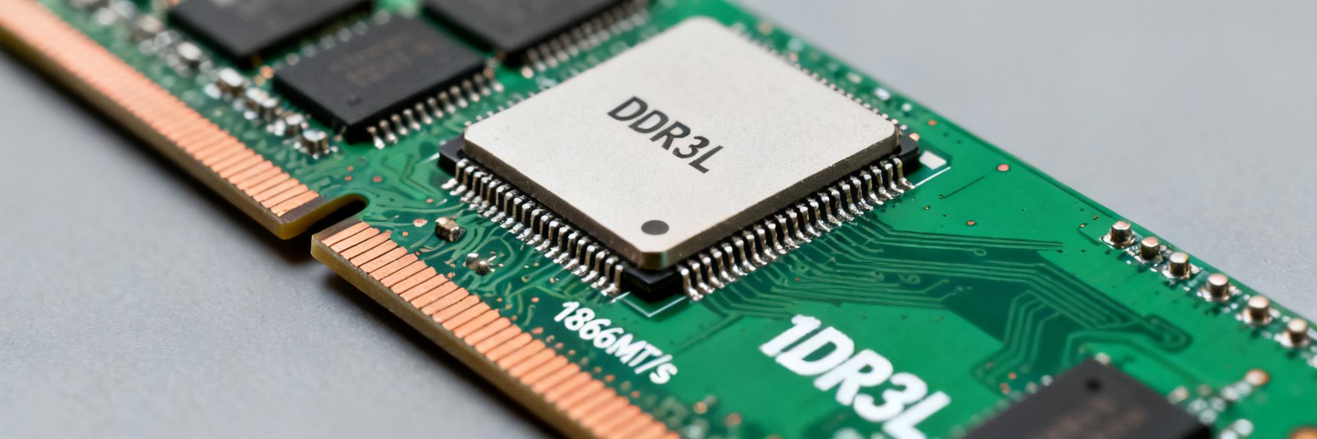
Point: The device is a 4 Gbit organized as 256M x16 in a 96-ball FBGA-style package suitable for DDR3L systems. Evidence: common DDR3L supply is nominally 1.35 V with an operating window allowing slight margining. Explanation: Typical speed grade is 1866 MT/s, available CAS options include CL11–CL13 families, and device temperature grades cover commercial to extended ranges—define scope for board SI and thermal planning.
- Capacity: 4 Gbit (256M x16)
- Package: 96-ball FBGA-style
- Speed grade: up to 1866 MT/s (933 MHz I/O)
- Typical Vdd: 1.35 V (DDR3L); margin per DDR spec
- Common CAS: CL11–CL13
Raw timing & speed points to use later in analysis
Point: JEDEC speed grade maps to key timing parameters used in calculations. Evidence: use 1866 MT/s with CL13 as a representative point—tCK ≈ 1.07 ns, CAS latency ≈ 13 cycles. Explanation: The theoretical peak bandwidth formula is MT/s × data width ÷ 8; for a 16-bit device at 1866 MT/s that yields ~3.73 GB/s. The table below contrasts spec vs. typical lab measures for baseline reference.
| Spec | Value | Typical Lab |
|---|---|---|
| Data rate | 1866 MT/s | 1850–1866 MT/s |
| CAS | CL13 | Measured 12.8–13.2 cycles equiv. |
| Peak bandwidth | ~3.73 GB/s | 3.3–3.6 GB/s sustained (seq) |
Throughput & Latency: Quantified Performance Metrics
Bandwidth calculations and real-world sustained throughput
Point: Peak device bandwidth is straightforward but sustained throughput varies with access pattern. Evidence: Peak = 1866 MT/s × 16-bit ÷ 8 = ~3.73 GB/s per device. Explanation: In multi-rank/channel systems, aggregate bandwidth scales by rank and channel count, but measured sustained throughput is typically 10–15% lower for sequential transfers and 40–60% lower for random patterns due to command overhead, precharge, and refresh effects.
Recommended presentation: show theoretical vs. measured for sequential read, random read, sequential write, and mixed 70/30 workloads. Use mean, stdev and percent of peak to help system architects budget performance headroom.
Latency breakdown and impact on application-level performance
Point: Effective application latency depends on CAS, tRCD, tRP, queueing, and refresh behavior. Evidence: CL13 at 1866 MT/s implies nominal device latency around 13×tCK; additional command-to-data timings add cycles. Explanation: Streaming workloads hide latency via prefetch and buffering; random-access and pointer-chasing workloads expose raw latency. Measure using repeatable random 4KB patterns and report tail percentiles (95th/99th) to capture real-world impact.
Power, Thermal Behavior & Accelerated Stress Data
Power vs. speed/voltage tradeoffs for DDR3L operation
Point: Power rises with frequency, toggling activity and slight Vdd increases. Evidence: At nominal 1.35 V, active current for comparable 4 Gbit DDR3L parts commonly shows a multi-tens of mA baseline with hundreds of mA under heavy toggling; small voltage shifts (±0.05 V) change energy per bit measurably. Explanation: Present power vs. frequency curves and compute energy-per-bit (mJ/GB) to make cost/thermal tradeoffs explicit for system-level thermal design.
Thermal & temperature-induced performance variation
Point: Temperature reduces timing margins and can increase BER. Evidence: Typical test points—0°C, 25°C, 85°C—show margin tightening at high temp and elevated corrected ECC events. Explanation: High-temperature operation shortens allowable tCK margins; track BER vs. temp and include recommended derating or slowed timing profiles for designs operating near upper thermal limits.
Yield, Reliability Drivers & Screening Considerations
Typical failure modes, DPPM and screening considerations
Point: Yield losses stem from wafer defects, packaging opens/shorts, and parametric outliers. Evidence: These fail as timing margin loss, stuck bits, or elevated BER during burn-in. Explanation: Use a simple yield math example—wafer yield × package yield × test yield → final DPPM—and show how small parametric shifts increase supply lead time and impact procurement acceptance thresholds.
Test coverage, burn-in, and binning strategies to improve field reliability
Point: Effective screening reduces escapes but costs time and yield. Evidence: Combine targeted margining, burn-in at voltage/temperature extremes, and ECC-log capture to identify marginal parts. Explanation: Recommend burn-in profiles (elevated temp and toggling), margin scans for tCK and Vdd, and logging of corrected events with sample-size guidance for acceptance (e.g., batches with N>100 with stratified sampling).
Benchmarking Methodology & Best Practices
Test setup, SI considerations & JEDEC-compliant procedures
Point: Repeatable SI and environmental control are essential. Evidence: Controlled impedance routing, proper termination, calibrated clock sources and fixture calibration yield consistent eye/timing measurements. Explanation: Before benchmarks, validate board impedance, reference clocks, and run an eye/timing sweep. Capture supply tolerance and ambient temperature for each run to allow apples-to-apples comparisons.
Benchmark suites, statistical sampling and data reporting templates
Point: Use standardized workloads and statistical reporting to compare designs. Evidence: Suggested workloads include sequential full-width read/write, random 4KB read/write, and mixed ratios; sample size N devices/runs ensures statistical power. Explanation: Report mean, stdev, min/max, percentile histograms, corrected/uncorrected error counts, and margin distributions so results can be aggregated across lots and sites.
Case Study: Diagnostics & System Optimization Checklist
Short case scenario: degraded throughput traced to timing margin loss
Point: Example: throughput fell 20% under thermal stress. Evidence: Margin scan showed tCK margin shrink by 0.12 ns and ECC events rose. Explanation: Root cause was routing-induced voltage droop; corrective steps included local decoupling, tightening Vdd regulation, rerouting high-speed traces, then validating recovery via repeated margin scans and workload reruns.
Designer checklist: system-level and manufacturing actions to improve performance & yield
Point: A concise checklist closes the loop between design, test and procurement. Evidence: Actions include validating DDR3L rails, SI layout checks, production margining, targeted burn-in, and ECC monitoring. Explanation: Quick mitigations—voltage margining, relaxed timing bins, rank/channel reconfiguration—should be specified with escalation criteria for test houses when corrected error trends exceed thresholds.
Summary / Conclusion
The MT41K256M16TW-107 delivers solid DDR3L bandwidth at 1866 MT/s with predictable latency and clear power/thermal tradeoffs, but real-world performance and availability depend heavily on voltage, temperature, and screening strategy. Top actions: adopt the recommended benchmarking methodology, implement systematic margining and burn-in, and apply the designer checklist to reduce escapes and improve shipped performance.
Key Summary Points
- MT41K256M16TW-107 offers ~3.73 GB/s peak per device at 1866 MT/s; measure sustained throughput with sequential and random patterns to define realistic performance budgets.
- Power rises with frequency and toggling; compute energy-per-bit and include thermal worst-case in system budgets to avoid timing-margin losses at high temperatures.
- Implement margin scans, burn-in, and ECC monitoring in production test to reduce DPPM and improve field reliability; document pass/fail criteria and sample sizes for procurement.
Common Questions & Answers
What are the expected MT41K256M16TW-107 performance benchmarks for sequential and random workloads?
Sequential read/write sustained throughput is typically 85–95% of peak in optimized paths (~3.2–3.5 GB/s), while random workloads often fall to 40–60% of peak due to activation/precharge and command overhead. Report percentiles and stdev to capture variability across devices.
How should engineers test MT41K256M16TW-107 DDR3L timing margins for production acceptance?
Run tCK margin scans across temperature and Vdd corners, capture ECC-corrected events, and define pass/fail based on minimum margin thresholds (e.g., margin > X ps) plus acceptable corrected-error limits. Use stratified sampling (N>100 for lot acceptance) and document test vectors and fixture calibration.
What practical steps reduce MT41K256M16TW-107 yield escapes and improve field performance?
Adopt targeted burn-in, tighten power rail decoupling, perform SI layout fixes, implement margining in production test, and monitor ECC trends. When corrected events climb, escalate to deeper binning/burn-in and consider conservative timing bins to protect customer deployments.
What is the theoretical peak device bandwidth of the MT41K256M16TW-107 and how is it calculated?
The theoretical peak bandwidth is ~3.73 GB/s. It is calculated using the formula: Data Rate (1866 MT/s) × Data Width (16-bit) ÷ 8 bits/byte = 3.732 GB/s.