MT41K256M16TW-107: تحليل متعمق للمواصفات الفنية والمؤشرات الرئيسية
The MT41K256M16TW-107 is a low-voltage, x16-organized 4Gb DDR3L device rated for DDR3-1866 operation (933 MHz clock / 1866 MT/s) at 1.35 V, offering a compact density option for embedded and industrial memory subsystems. This article provides a hands-on, metric-focused breakdown to help engineers decide if MT41K256M16TW-107 fits their design by translating datasheet numbers into power, timing, and SI targets for real boards.
Readers will find a logical organization guide, electrical/timing extraction workflow tied to the DDR3L datasheet, throughput calculations (peak and realistic), PCB and PDN recommendations, and a procurement-ready validation checklist to run before committing to qualification.
1 — Product overview: What MT41K256M16TW-107 is and where it fits
— Logical organization & capacity
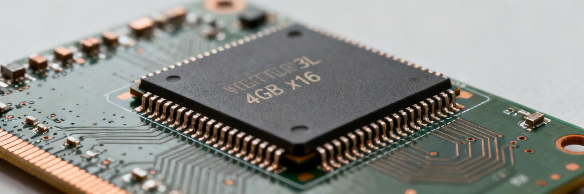
Organization is 256M × 16 = 4Gb (4 gigabit) presented as multiple banks and the effective row/column addressing determined by the device geometry. The x16 data bus means each transfer moves 16 bits; paired with a dual-data-rate interface this suits controllers that expose 16-bit channels or that aggregate two x8 devices. Designers prefer x16 for simpler routing in single-device channels and when controller ports are native x16; x8 is chosen when byte-level ECC or more flexible channel interleaving is required.
— Package, temperature grade & voltage class
This part ships in an FBGA-style ball-count package optimized for dense layouts; its DDR3L classification at 1.35 V reduces active power versus 1.5 V parts and supports extended temperature grades used in industrial modules. Board-level implications include tighter BGA soldering control, thermal via planning, and ensuring assembly profiles accommodate the package ball-count and temp grade when reflowing modules. Quick spec bullets below summarize core attributes for reference.
| Parameter | Value |
|---|---|
| Density | 4Gb (256M × 16) |
| Speed grade | DDR3-1866 (933 MHz clock / 1866 MT/s) |
| Voltage | 1.35 V (DDR3L) |
| Organization | x16 |
| Package | FBGA (BGA ball-count) |
2 — Electrical & timing spec deep-dive (key datasheet metrics)
— Core electrical characteristics
Key rails are VDD and VDDQ at 1.35 V; VREF typically sits at VDDQ/2 for termination and VTT is used only if register termination or explicit VTT is required by the controller. Datasheet active and standby currents are given as ranges—active currents (ICC0/ICC1) might span tens to low hundreds of mA depending on access pattern; standby currents drop to single-digit mA in deep power-down. Convert to system watts by multiplying current by 1.35 V and summing across devices and rails to budget PDN headroom and thermal dissipation.
— Timing parameters to extract from the datasheet
Extract CAS latency (CL), tRCD, tRP, tRAS, tRC and tFAW from the timing tables for the target speed grade. These define command-to-data windows and constrain achievable throughput. Use the formula: latency_ns = (cycles / (MT/s / 1000)) to convert cycles to ns (for example, CL at 1866 MT/s: ns = CL / 933). Record these values to ensure your controller timing engine can meet required margins under temperature and voltage variation.
3 — Performance & throughput: real-world metrics and calculations
— Theoretical bandwidth and practical throughput
Peak bandwidth = (MT/s × data width) / 8. For 1866 MT/s and x16: (1866 × 16) / 8 = 3732 MB/s peak per device. Realistic throughput is lower: account for refresh (~3–5% time), bank conflicts, and controller overhead; expect sustained 60–80% of peak in well-optimized systems, i.e., ~2.2–3.0 GB/s. Use this worksheet: peak_MBps = (MTs × width)/8; sustained_MBps = peak_MBps × efficiency_factor (0.6–0.8).
Peak example: 1866 MT/s × 16 bits → (1866×16)/8 = 3732 MB/s. At 70% efficiency → ~2,612 MB/s sustained.
— Latency vs. bandwidth trade-offs and benchmarking pointers
Translate CL and tRCD into absolute read latency (ns) using the earlier formula; lower CL reduces access latency but may demand tighter SI and faster controller clocks. Benchmark patterns: sequential burst to measure peak streaming, small random 32–64B accesses to stress latency, and page-open tests to reveal bank-conflict behavior. Capture read/write latency distributions, sustained MB/s, and bank conflict rate to validate suitability for target workloads.
4 — PCB, signal-integrity & power delivery guidelines for DDR3L designs
— Routing, termination and layout best practices
At a 933 MHz clock, controlled impedance (typically 50 Ω single-ended), trace length matching (DQ to DQ and DQS strobe matching), and minimal via count are essential. Aim for DQ group length matching within ~50–100 ps skew and DQS center-to-center matching to DQ byte lanes. Use on-die and parallel termination strategies per controller guidance and route DQS as a paired route to minimize crosstalk and maintain timing.
— Power sequencing, decoupling and thermal handling
Follow required VDD/VDDQ sequencing—often VDD precedes VTT/VREF—and verify ramp slopes meet datasheet limits to avoid latch-up. Employ a decoupling network with bulk (10–47 μF), mid (0.1–1 μF), and high-frequency (0.01 μF) caps placed close to BGA power balls. For extended temp grades, provide thermal vias beneath the package and validate worst-case self-heating during sustained high-activity patterns.
5 — Selection, validation & procurement checklist (making go/no-go decisions)
— Datasheet comparison & grade variants
Compare candidate parts across speed grade, CAS/timing, voltage class, package, and temperature range; confirm each item against the DDR3L datasheet table. Use the checklist table below to capture attributes per lot so validation teams can quickly spot mismatches and maintain traceability during qualification.
| Attribute | Candidate A (MT41K256M16TW-107) | Candidate B |
|---|---|---|
| Speed (MT/s) | 1866 | 1600 |
| CL / tRCD / tRP | 11 / 11 / 11 | 9 / 9 / 9 |
| Vdd | 1.35 V | 1.5 V |
| Temp range | -40 to 85°C | -40 to 95°C |
— Testing, qualification and compatibility checks
Recommended procedures: power-up sequencing tests, JEDEC conformance-like patterns, long-duration stress (walking ones/zeros, address hammering), and thermal cycling. Order validation samples (typ. ≥10 units per lot) with lot/date codes and document pass/fail criteria for timing margins, PDN stability, and sustained throughput before volume procurement.
Summary
- MT41K256M16TW-107 provides a compact 4Gb DDR3L x16 option suitable for low-voltage, moderate-to-high-speed embedded and industrial systems; confirm package and temp grade for assembly and thermal plans.
- Key verifications: timing (CL, tRCD, tRP), core and I/O currents to estimate system power, and SI targets for 933 MHz clocking to secure acceptable latency and throughput.
- Action: run the supplied checklist and throughput worksheet under worst-case thermal and PDN conditions to validate margins before procurement.
FAQ
What key DDR3L datasheet items should I verify for MT41K256M16TW-107?
Verify speed grade tables, timing parameters (CL, tRCD, tRP, tFAW), voltage and VREF specs, maximum allowed toggle rates, and current consumption ranges. These determine controller timing setup, PDN sizing, and thermal design margins; capture them in a comparison spreadsheet per lot for qualification.
How do I estimate system power from the datasheet numbers?
Take active and standby current figures from the datasheet, multiply by 1.35 V to get per-device power, then multiply by device count and add controller/regulator losses. Include refresh and average activity factors (use measured activity percent) to convert peak currents into realistic sustained power.
Is an x16 organization appropriate for ECC or multi-channel controllers?
x16 simplifies routing and suits single-channel controllers; for systems requiring byte-level ECC or finer interleaving, x8 devices are typically preferred. Match organization to controller capabilities and ECC requirements during early component selection to avoid redesign.
What are the PCB impedance and skew matching tolerances for DDR3-1866 routing?
For DDR3-1866 (933 MHz), target single-ended trace impedance at 50 ohms (±10%) and differential impedance (DQS/CLK) at 100 ohms (±10%). DQ-to-DQS skew must be matched within ±10 ps (approx. ±0.6mm in FR4), and Address/Command-to-CLK within ±25 ps.