ورقة بيانات MX25L25645GM2I-08G: المواصفات الكاملة وتخطيط الأطراف
The MX25L25645GM2I-08G is a 256-Mbit serial NOR flash device offering multiple SPI modes, typical clock support up to high-speed SPI frequencies, and a nominal VCC operating range that targets low-power embedded systems. This article extracts measurable takeaways from the official datasheet and provides a concise, actionable reference of complete specs and the full pinout for fast integration, including timing, electrical bounds, and integration tips.
Product Overview & Key Features
Overview & Intended Use
The device is a serial NOR flash memory family member optimized for code and data storage. It supports single, dual, and quad SPI modes and has a density class suitable for firmware images and data logging. Designers typically use it for firmware storage, code shadowing (XIP), and nonvolatile logs where read throughput and low standby power are priorities; MX25L25645GM2I-08G balances capacity and performance.
Summary of Top-Line Specs
For quick decisions during part selection and footprint review, refer to the core structural parameters listed in the reference table below.
| Spec Parameter | Value / Range (Typical Bounds) |
|---|---|
| Capacity | 256 Mbit (32 Megabytes) |
| Interfaces | Standard SPI, Dual SPI, Quad SPI (MXSMIO) |
| Operating VCC Range | 2.7V to 3.6V (Nominal 3.0V/3.3V rails) |
| Temperature Range | Industrial Grade (-40°C to +85°C) |
| Standard Package | 8-SOP (200mil) / 8-WSON (8x6mm) |
Electrical & Timing Specifications
Electrical Characteristics
To ensure robust power delivery and protect internal structures, engineers must design power stages around strict electrical bounds. The following table identifies maximum limits, active current metrics, and standby modes under specific operational conditions.
| Electrical Metric | Minimum Bound | Typical Value | Maximum Limit |
|---|---|---|---|
| Supply Voltage (VCC) | 2.7V | 3.0V / 3.3V | 3.6V |
| Active Read Current (ICC1) | — | 15 mA | 25 mA (at 133MHz) |
| Active Program/Erase Current | — | 18 mA | 30 mA |
| Standby Current (ISB) | — | 40 µA | 80 µA |
| Deep Power-Down Current (IDPD) | — | 1.5 µA | 15 µA |
Timing Parameters & Performance
Timing critical bounds define system speed and flash transaction responsiveness. Achieving peak performance in high-speed read modes requires strict adherence to maximum clock limitations and programmatic latency configurations.
- Maximum SCLK Frequency (Normal Read): 50 MHz
- Maximum SCLK Frequency (Fast Read / Quad): Up to 133 MHz
- Page Program Time: 0.33 ms (typical, 256 bytes)
- Sector Erase Time (4KB): 25 ms (typical)
- Block Erase Time (64KB): 0.45 s (typical)
Full Pinout & Package Information
Pin Assignment with Signal Descriptions
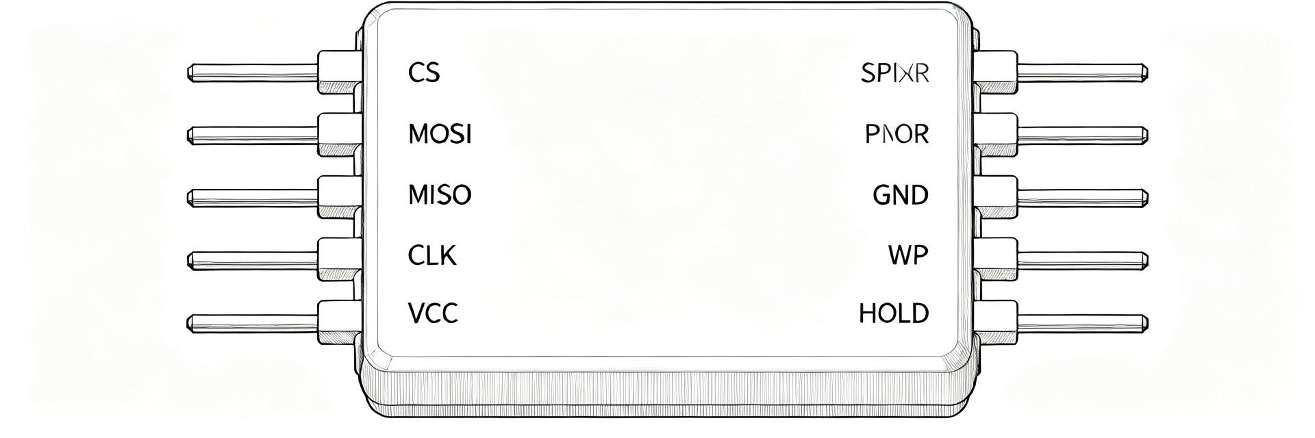
The standard 8-pin mapping handles dual and quad multi-I/O configurations by repurposing standard write protect and hold lines for data signals. Ensure high-frequency layout techniques are applied to clock and data traces to prevent signal integrity degradation.
- CS# (Chip Select): Active low input pin used to activate and frame SPI operations.
- SO/SIO1 (Serial Data Output / Serial I/O 1): Outputs data in standard SPI mode. Used as an bidirectional input/output pin in Dual/Quad modes.
- WP#/SIO2 (Write Protect / Serial I/O 2): Provides hardware write protection. Configured as bidirectional I/O in Quad mode.
- GND (Ground): Reference zero potential node. Must connect directly to a solid ground plane.
- SI/SIO0 (Serial Data Input / Serial I/O 0): Inputs instructions, addresses, and data. Configured as bidirectional I/O in Dual/Quad modes.
- SCLK (Serial Clock Input): Synchronizing clock input. Keep traces as short and clear as possible.
- HOLD#/SIO3 (Hold Input / Serial I/O 3): Pauses serial operations without deselecting the device. Configured as bidirectional I/O in Quad mode.
- VCC (Power Supply): Main voltage supply pin. Place decoupling passives immediately adjacent to this node.
Functional Blocks & Command Set Overview
Core Functions and Operation Modes
The system utilizes a memory array state engine supporting standard sequential reads and high-speed multi-I/O transactions. Built-in protection blocks lock designated memory segments using status register bits. Execute-in-Place (XIP) configurations rely heavily on low-latency Quad SPI modes to fetch code instructions directly without prior RAM shadowing.
Command Set Essentials & Integration Code
Standard SPI transactions use specific 8-bit opcodes to drive memory operations. Below is a list of key command hex values and a code example for a standard Fast Read command sequence.
- Read Array (Normal): 0x03
- Fast Read (High Speed): 0x0B
- Write Enable (WREN): 0x06
- Sector Erase (4KB): 0x20
- Page Program: 0x02
// Pseudo-code: Fast Read Sequence (XIP Example)
void Flash_Fast_Read(uint32_t address, uint8_t* buffer, uint32_t length) {
    CS_LOW();
    SPI_TRANSFER(0x0B);                 // Fast Read Command Opcode
    SPI_TRANSFER((address >> 16) & 0xFF); // Address [23:16]
    SPI_TRANSFER((address >> 8) & 0xFF);  // Address [15:8]
    SPI_TRANSFER(address & 0xFF);         // Address [7:0]
    SPI_TRANSFER(0x00);                 // Dummy Cycle (Requires 8 clocks)

    for (uint32_t i = 0; i < length; i++) {
        buffer[i] = SPI_TRANSFER(0xFF); // Receive data bytes
    }
    CS_HIGH();
}
Reference Circuits & PCB Layout Integration
Reference Schematic & Component Recommendations
For high-frequency stability, place a low-ESR 0.1µF decoupling capacitor in parallel with a 1µF ceramic capacitor directly at the VCC pin. Place 10Ω to 47Ω damping resistors close to the controller on the SCLK, SI, and SO lines to prevent transmission line reflections and ringing. Always tie WP# and HOLD# to VCC through 10kΩ pull-up resistors if their hardware control features are not used in your application design.
PCB Layout & Signal Integrity Checklist
- Route the SCLK line with the shortest, most direct trace possible. Do not run it parallel to high-noise traces or switching nodes.
- Implement a continuous reference ground plane beneath the flash and its high-speed signals.
- For WSON packages, use thermal ground stitching vias under the exposed central pad to optimize thermal dissipation.
- Set up the power-up sequence to keep CS# high, tracking VCC, to prevent accidental writes before the system voltage stabilizes.
Validation, Selection Checklist & Documentation Tips
Production & Testing Checklist
- Measure actual VCC rise times during power-on to ensure they do not violate the datasheet’s minimum start-up thresholds.
- Verify timing margins on the SCLK, CS#, and SPI data lines with an oscilloscope at maximum operating temperature.
- Implement high-temperature write and erase verification cycles during FAE validation to confirm memory endurance.
- Utilize AOI (Automated Optical Inspection) and X-ray tools during production to verify package coplanarity and solder fillet quality.
Conclusion
For successful system integration, engineers should confirm operational voltage and logic levels, validate SPI timing and mode support, and review the full pinout and land pattern before PCB release. Use the official datasheet as the final authority and run early bench tests on the reference schematic for successful integration of the MX25L25645GM2I-08G.
Key Summary
- High-Density Capacity: The MX25L25645GM2I-08G provides 256-Mbit of storage. Dual and Quad SPI interface modes significantly increase read throughput.
- Strict Timing Budgets: Ensure your controller matches high-frequency parameters up to 133 MHz. Keep trace lengths matched to prevent skewing.
- Layout Best Practices: Always isolate clock traces, place decoupling capacitors close to VCC, and verify power-up timing sequences to prevent corruption.
Frequently Asked Questions
How should engineers verify the device's SPI timing?
Engineers should reproduce datasheet test conditions in the lab, use a logic analyzer to capture CS#, SCLK, SI, and SO timing, and validate margins by sweeping clock frequency and observing read/write success rates. Always document typical versus worst-case timing for system validation.
What are common PCB footprint mistakes to avoid?
Common errors include insufficient decoupling placement, missing thermal pad vias (if applicable), incorrect pad dimensions, and long SCLK traces. Validate the land pattern against the mechanical drawing and perform DRC checks with recommended solder mask clearances.
Which tests are critical during production validation?
Critical production tests cover power sequencing verification, SPI functional tests (read/program/erase), endurance sampling, solder joint X-ray or AOI inspections, and in-system boot tests to ensure reliable firmware loading and stability in target operational modes.
What is the recommended power-up sequencing for the MX25L25645GM2I-08G?
To prevent unintended write operations during power-up, keep CS# high tracking VCC. A minimum delay (tVSL) is required after VCC reaches its minimum operating voltage before initiating any SPI commands.