GD5F1GQ5UE datasheet: Key Specs & Performance Breakdown
Modern SPI NAND devices deliver higher density and integrated error management while shrinking BOM and boot time impacts for embedded designs. This article focuses on the GD5F1GQ5UE datasheet, outlining the device’s density, interface modes, ECC behavior and endurance so embedded storage designers and system engineers can assess suitability for firmware, logging and OTA update roles.
Scope: this write-up interprets datasheet fields and shows system-level implications; it does not reprint the full specification or replace hands‑on lab validation. Key takeaways previewed: 1 Gb density, QSPI-compatible interface, on‑media ECC, and moderate P/E endurance targets that affect lifetime modeling.
Background: What GD5F1GQ5UE Is and Where It Fits
Device overview and positioning
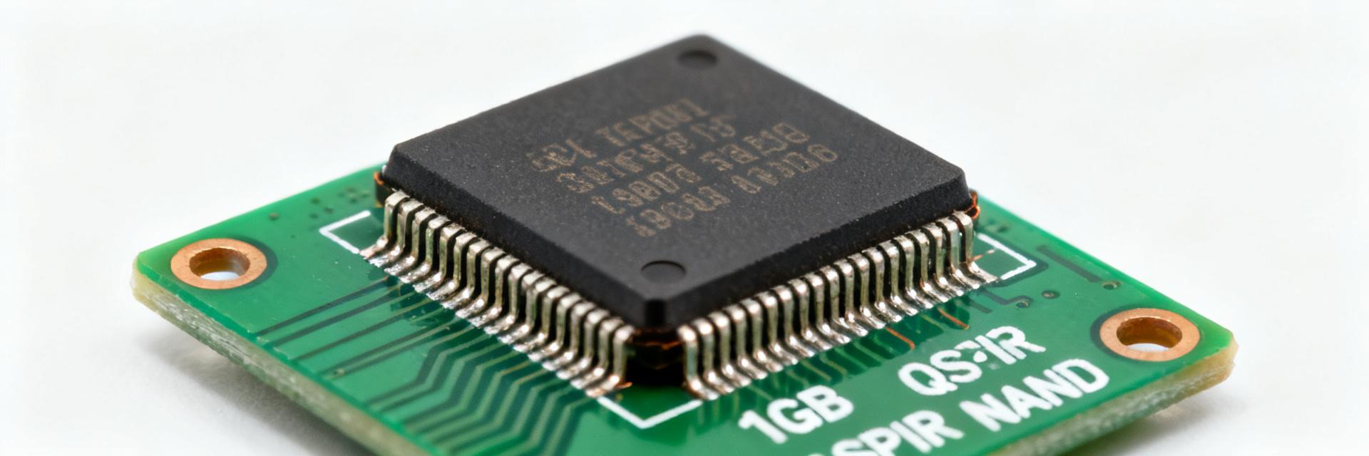
Point: The device is a single‑chip SPI/quad‑SPI NAND intended for embedded code and data storage. Evidence: Datasheet entries list 1 Gbit density, serial x1/x2/x4 read modes and single‑chip packages with 3.3 V nominal supply. Explanation: That profile places it between small NOR code stores (low latency) and parallel NAND (high throughput), making it a compact option for boot images, firmware and moderate bulk data.
Why these NAND choices matter for system design
Point: Choosing serial NAND affects latency, controller complexity and board area. Evidence: The datasheet’s documented page sizes, program/erase timings and ECC expectations are the key NAND flash specs engineers must compare. Explanation: On‑chip ECC and QSPI modes reduce host CPU ECC burden and pins, but designers trade off slightly higher random read latency versus parallel NAND; that trade influences boot time and controller selection.
Datasheet Snapshot: Key Specs at a Glance
Point: Quickly capture the fields that determine electrical compatibility and mechanical fit. Evidence: The GD5F1GQ5UE datasheet lists density, voltage ranges, temperature grade, package options, I/O counts and recommended operating ranges. Explanation: Those numbers answer whether the part fits a given MCU domain, board footprint and industrial temperature requirement before deeper timing analysis.
Electrical & physical specs to capture immediately
Point: Extract VCC/VIO, operating temperature, package and pin count first. Evidence: Typical datasheet values include VCC 3.0–3.6 V nominal with VIO options, commercial/industrial temperature grades, and single‑row WSON or SO packages with 8 I/O contacts. Explanation: These values define level shifting need, decoupling strategy and whether the part meets an assembly’s thermal and mechanical constraints.
| Parameter | Typical Value |
|---|---|
| Density | 1 Gbit |
| Supply (VCC) | 3.0–3.6 V |
| IO modes | x1, x2, x4 (QSPI/quad) |
| Temp grade | Commercial / Industrial options |
| Package | Small serial packages (eg. 8 I/O) |
Interface modes & protocol highlights
Point: Supported SPI and QPI modes determine peak throughput and required command sequences. Evidence: The datasheet documents x1/x2/x4 read modes, QPI capability, maximum clock rates and required dummy cycles for each mode. Explanation: Use quad modes at higher MHz to minimize sequential read time for boot images; note command timing windows and voltage-level timing to avoid bus contention.
Performance Breakdown: Throughput, Latency & Power
Measured and datasheet throughput & latency (read/program/erase)
Point: Datasheet sequential read bandwidth and page program/erase times translate to system boot and update durations. Evidence: Sequential read in quad mode at a given clock yields x MB/s (per datasheet clock table); typical page program and block erase times are listed in ms. Explanation: For example, a 256 KB boot image read at 50 MHz quad (approximate effective throughput) yields an expected read time in the tens of milliseconds — useful for estimating boot‑from‑flash latency.
Power consumption and timing trade-offs
Point: Clock rate and I/O width drive active current; standby currents enable deep sleep budgets. Evidence: The datasheet provides active, I/O and standby current figures for each mode and voltage level. Explanation: For low‑power designs prefer x1 low‑clock reads for occasional access and use deep standby between bursts; validate by measuring current with the target MCU and board parasitics to confirm battery life projections.
Integration & Implementation Guide
Pinout, signal integrity and electrical connection tips
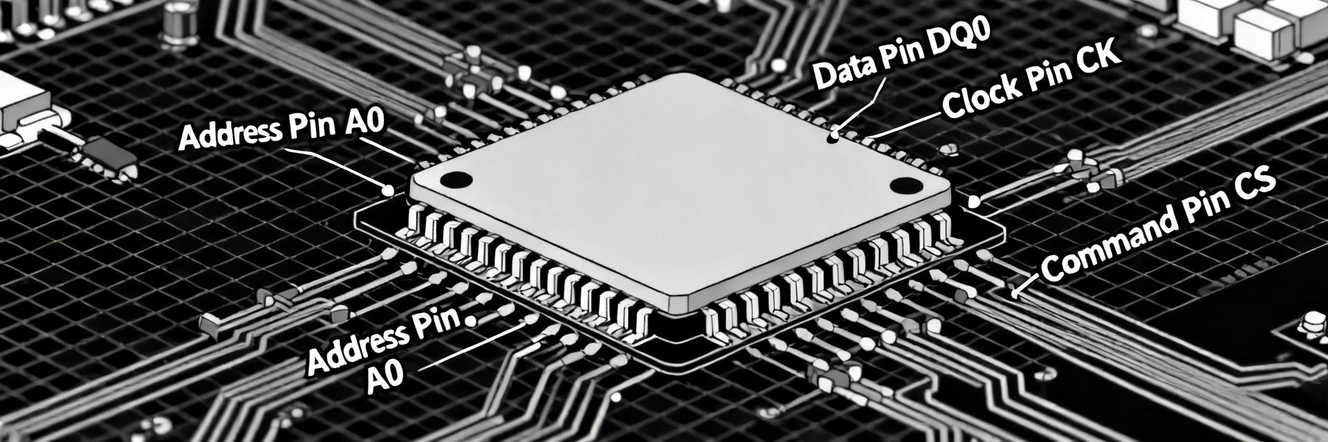
Point: Proper routing and level handling avoid signal glitches at multi‑MHz transfers. Evidence: Key pins documented include CE#, CLK, IO0‑IO3, RESET/HOLD and VCC/VIO rails. Explanation: Route CLK with matched length to IO lines where possible, place a 0.1 µF decoupler near VCC, and add level shifters if MCU I/O is 1.8 V while flash VIO is 3.3 V to prevent damaging voltages.
Command sequences, driver notes & boot considerations
Point: Implement standard read/fast read and status‑poll sequences, and honor required dummy cycles. Evidence: The datasheet specifies command opcodes, required inter‑command delays and status register polling bits. Explanation: A typical boot flow sends read‑setup, waits configured dummy cycles, reads pages and polls status; firmware should implement retries and handle busy windows to avoid corrupted boot images.
Reliability, Endurance & Error Management
P/E cycles, data retention, bad block management
Point: Endurance and retention specs define usable lifetime under write workloads. Evidence: The datasheet lists program/erase cycle ratings and expected data retention under specified temperatures. Explanation: Model lifetime by combining average daily written volume with P/E rating and include bad‑block tracking and spare management to maintain capacity over time.
On‑chip ECC vs system ECC and implications for design
Point: On‑chip ECC reduces host complexity but defines correctable bit‑flip limits. Evidence: Datasheet ECC notes indicate media‑level error correction capability per page and how uncorrectable errors are reported. Explanation: Rely on on‑chip ECC for typical flip rates; for high‑reliability designs add system‑level checks (CRC, redundancy or higher‑level RAID) and run accelerated wear tests to validate error behavior.
Use Cases, Comparisons & Practical Selection Checklist
Example use cases and design choices
Point: Map device strengths to real embedded scenarios. Evidence: The device’s density, QSPI modes and on‑chip ECC make it suited for firmware/boot storage, circular data logging and moderate bulk read archives. Explanation: Use it for compact boot images and OTA metadata; for continuous high‑write logging consider higher P/E endurance alternatives or implement wear leveling and rolling logs to extend life.
Quick selection checklist & trade‑off table
| Question | Action |
|---|---|
| Required density? | Confirm 1 Gbit covers firmware and headroom. |
| Interface speed? | Specify x4/QPI and target MHz to meet boot time. |
| Endurance needs? | Compare P/E cycles to expected daily writes. |
| ECC requirements? | Decide on on‑chip vs system ECC layers. |
| Temperature & package? | Choose industrial temp grade and package pinout. |
Summary
Point: The GD5F1GQ5UE datasheet presents a compact SPI NAND option with 1 Gb density, quad SPI modes and media‑level ECC suitable for many embedded boot and logging roles. Evidence: Key datasheet fields show VCC/VIO, timing, ECC and endurance figures that determine fit. Explanation: Designers should validate timing windows, power trade‑offs and endurance under realistic workloads before production acceptance.
Key Summary
- The device offers 1 Gbit density with x1/x2/x4 interface modes; verify VCC/VIO and package match system power and footprint constraints.
- On‑chip ECC simplifies host design but imposes media‑level correctable limits; plan system CRC or redundancy for high‑reliability use cases.
- Throughput and latency scale with clock and I/O width; use quad mode for faster boot reads and lower clock for power‑sensitive operations.
- Model lifetime from P/E cycles and daily write volume, and implement bad‑block management and wear leveling in firmware.
Frequently Asked Questions
What does the GD5F1GQ5UE datasheet specify about endurance and P/E cycles?
The datasheet provides a program/erase cycle rating for the media and expected data retention under specified temperatures; use those figures to calculate lifetime by multiplying average daily writes by bytes per program. Implement bad‑block tracking and spare management to tolerate blocks that degrade earlier than average.
How does the GD5F1GQ5UE datasheet define on‑chip ECC behavior?
The datasheet documents the on‑media ECC correction capability per page and how uncorrectable errors are indicated in status registers. Designers should rely on that ECC for typical flip rates, but validate with accelerated BER tests and add higher‑level checks (CRC/redundancy) in systems with very low tolerance for data loss.
Can the GD5F1GQ5UE datasheet guide boot time estimates for an embedded image?
Yes—use the documented maximum clock rate, quad read effective throughput and page read times to estimate sequential read durations. For example, compute image size divided by effective MB/s in quad mode and add program/erase overheads for update scenarios to estimate boot and OTA update times.
What are the key electrical constraints for integrating GD5F1GQ5UE?
The device operates at VCC 3.0–3.6 V nominal. If your MCU I/O voltage is lower (e.g., 1.8 V), you must implement level shifters to prevent damage. Proper decoupling capacitors (0.1 µF) near the VCC pin are essential for stable multi-MHz transfers.