GD5F2GM7UEYIGR Datasheet Deep Dive: Specs & Benchmarks
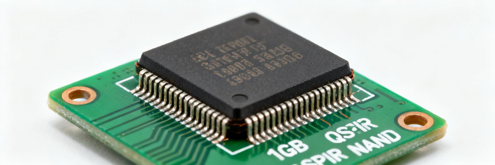
Point: The GD5F2GM7UEYIGR datasheet presents a compact 2Gb SLC SPI NAND device aimed at embedded boot and moderate-write storage roles.
Evidence: The datasheet specifies a 133 MHz maximum clock, support for SPI x1/x2/x4 interfaces and integrated on-chip ECC.
Explanation: This combination targets low-latency firmware loads and reliable small-block storage where controller complexity and board area are constrained, so designers must map datasheet claims to measured throughput and endurance before committing to production.
1 — Quick technical snapshot (background)

Point: Key electrical and memory specs summarize operational constraints designers need first.
Evidence: Typical values include 2Gb SLC density, supply nominally in the 2.7–3.6 V window, industrial operating temperature ranges, and small-package pin counts suitable for 8–16 pin QFN/TSOP options.
Explanation: These specs imply straightforward power rails for 3.3 V systems, simple BOM changes for industrial-grade parts, and package choices that balance PCB area and thermal dissipation during program/erase cycles; designers should confirm package thermal resistance against expected P/E activity.
Key electrical & memory specs
Point: Interface and signaling define achievable bandwidth and integration effort.
Evidence: The device supports SPI single/dual/quad I/O modes, optional DTR, and a maximum SCLK of 133 MHz.
Explanation: In practice, quad I/O at 133 MHz gives the best throughput for read-heavy paths while single-bit SPI eases legacy MCU support; selection impacts controller DMA needs and board-level signal integrity, so pick modes aligned with the host’s IO capability.
Functional building blocks & on-chip features
Point: On-chip architecture and ECC behaviour determine reliability and host responsibilities.
Evidence: The chip implements internal ECC (multi-bit correctable), a page/block architecture with OOB/spare bytes for metadata, and block-erase units consistent with NAND paradigms.
Explanation: On-chip ECC reduces host overhead for correctable errors, but hosts must still track ECC reports and manage uncorrectable events through bad-block mapping, and reserve spare bytes for FTL data and wear metadata.
| Spec | Value (typical) |
|---|---|
| Density | 2Gb SLC |
| Voltage | 2.7–3.6 V |
| Max Clock | 133 MHz |
| Interface | SPI x1/x2/x4, DTR/Quad |
| Package | Small QFN/TSOP options |
2 — Performance benchmarks & throughput estimates (data analysis)
Point: Theoretical bandwidth and real-world throughput diverge unless measured carefully.
Evidence: Throughput can be estimated as SCLK × I/O width ÷ 8 × protocol efficiency; at 133 MHz quad I/O theoretical raw throughput approaches 66 MB/s before protocol overhead.
Explanation: Expect sustained application-level throughput 10–30% below theory depending on command overhead, small-transfer penalties, and controller buffering; validate with a test harness that issues long sequential reads to measure streaming and small random reads to measure IOPS.
Sequential & random throughput: how to calculate and measure
Point: Clear measurement methodology yields repeatable numbers.
Evidence: Use a host with DMA-capable SPI or an FPGA-based controller, capture SCLK/IO traces with a logic analyzer, and compute MB/s from transferred bytes over observed active SCLK windows.
Explanation: Ensure test firmware disables host caching and uses raw command sequences; measure x1 and x4 modes separately and include repeated long-read runs to average out thermal throttling effects.
Latency, program/erase timings & realistic IOPS
Point: Datasheet P/R/E timings convert to practical IOPS limits.
Evidence: Typical device program and erase times imply single-page program on the order of milliseconds and block erase tens of milliseconds, which limit sustained random-write IOPS without multi-plane parallelism.
Explanation: Micro-benchmark single-page program latency, sequential streaming writes, and small random writes to derive realistic IOPS; look for controller-side buffering or write-combining that may mask true device latency during short tests.
3 — Reliability, ECC & data integrity (data analysis)
Point: ECC behavior and error reporting frame the integrity model for field deployments.
Evidence: On-chip ECC reports correctable vs uncorrectable events via status bits; spare/OOB bytes and ECC counters allow hosts to log correction counts.
Explanation: Firmware should sample ECC counters frequently, flag rising correction rates as early-warning for wear, and escalate to remapping or overprovisioning when uncorrectable events approach defined thresholds.
On-chip ECC behavior and error-rate expectations
Point: Knowing correctable thresholds is essential for meaningful diagnostics.
Evidence: The device reports per-operation ECC status and supports multi-bit correction up to a vendor-defined limit; hosts must interpret these flags when deciding to rewrite or retire blocks.
Explanation: Induced bit-error testing across patterns and temperatures provides realistic BER curves; track corrected-bit distributions rather than only uncorrectable counts for predictive maintenance.
Endurance, retention, and thermal margins
Point: Translate cycles and retention into lifetime models for target workloads.
Evidence: Endurance (P/E cycles) and retention specs convert to usable life given daily write intensity; higher-temperature operation accelerates wear and retention loss.
Explanation: Model lifetime as (rated cycles × capacity) ÷ daily written bytes with margin; validate via accelerated P/E cycles and high-temp retention bakes to confirm endurance expectations under expected duty cycles.
4 — Integration & hardware design considerations (method guide)
Point: Power and signal integrity choices determine reliability at 133 MHz.
Evidence: Recommended decoupling includes local 0.1 µF and 1 µF caps near VCC pins, single-point ground, and controlled impedance SPI traces.
Explanation: Proper bypass placement reduces VCC dips during program pulses, and short matched-length traces with series termination resistors prevent ringing and EMI; validate with scope captures during high-activity bursts.
Power, decoupling & signal integrity
Point: PCB layout affects both signal fidelity and EMI.
Evidence: Place decoupling caps within 2 mm of device power pins, use solid ground pours, and route SPI IO with consistent impedance.
Explanation: These measures minimize timing jitter and reduce the chance of corrupted transfers at high SCLK; perform SI checks with eye diagrams captured on representative boards.
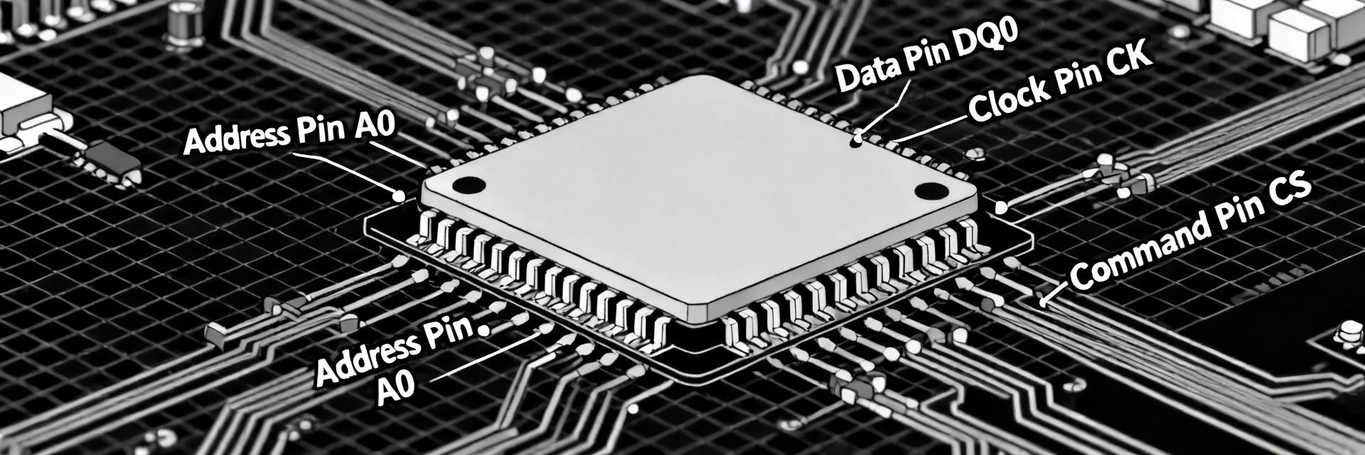
PCB footprint, pin mapping & package notes
Point: Footprint and reflow considerations reduce assembly risk.
Evidence: Use recommended land patterns, add test pads for CS and IO signals, and follow vendor reflow profiles for small-pin-count packages.
Explanation: Test pads enable in-system programming and failure analysis; ensure pin-mux conflicts on the host are resolved so CS and hold/reset signals can be tri-stated during boot.
5 — Firmware & software implementation checklist (method guide)
Point: Robust firmware handles initialization, mode switching, and error management.
Evidence: Canonical flows include device reset, read ID, enabling quad/DTR modes via mode-register writes, status polling after program/erase, and careful timing adherence.
Explanation: Implement retries with exponential backoff for transient errors, persist ECC and P/E counters to nonvolatile logs, and gate mode switches behind status confirmations to avoid bus lockups.
Initialization, command sequences & read/write flows
Point: Command timing and status handling are the backbone of reliable IO.
Evidence: Use documented reset, read-ID, read, program and erase sequences with status polling; confirm mode bits before issuing quad transfers.
Explanation: Firmware should include conservative status-poll timeouts and fallbacks to single-bit SPI to recover from misconfigured mode states during field updates.
Wear-leveling, bad-block management & ECC handling
Point: Simple mapping layers enable long-term reliability on SLC SPI NAND.
Evidence: Maintain a Bad Block Table (BBT), implement log-structured mappings for small writes, and perform periodic scrubbing to shuffle marginal blocks.
Explanation: Treat recoverable ECC spikes as precursors to block retirement, keep metadata in protected areas, and expose telemetry for field diagnostics to aid root-cause analysis.
6 — Benchmarks comparison & ideal use cases (case display)
Point: Positioning against class peers clarifies tradeoffs.
Evidence: Compared to similar 2Gb SLC SPI NAND devices, the GD5F2GM7UEYIGR-class part balances mid-range max clock and integrated ECC to favor cost-effective firmware storage.
Explanation: This part typically delivers favorable performance-per-cost for boot images and moderate logging but is less suitable for very high write-rate data logging without an advanced FTL.
How GD5F2GM7UEYIGR-class 2Gb SLC SPI NAND typically compares
Point: Comparative axes highlight selection priorities.
Evidence: Key axes—density, interface modes, max clock, P/E times, endurance—show this class is optimized for reliability and low latency rather than maximal throughput.
Explanation: Use anonymous performance/cost comparisons to decide if the part meets system targets; factor in host complexity and firmware overhead when comparing alternatives.
Best-fit applications and workload profiles
Point: Not all storage roles suit SLC SPI NAND equally.
Evidence: Ideal uses include boot/firmware storage, configuration blobs, and moderate-write logs; avoid raw high-intensity user-data logging without wear-leveling.
Explanation: For constrained systems requiring small-footprint reliable storage, this class offers a strong compromise between endurance, size, and integration effort.
7 — Validation & deployment checklist (action suggestions)
Point: A compact validation plan reduces field surprises.
Evidence: Pre-production should include datasheet cross-checks, electrical smoke tests, throughput and latency benchmarks, sampled endurance P/E cycles, and thermal cycling.
Explanation: Define acceptance criteria such as throughput within an acceptable percent of measured theoretical and uncorrectable ECC rates below threshold; implement production telemetry for P/E counts and ECC growth to catch issues early in the field.
Conclusion / Summary
- GD5F2GM7UEYIGR-class devices provide 2Gb SLC capacity with on-chip ECC and 133 MHz SPI, making them suitable for boot/firmware storage and moderate-write embedded roles.
- Run targeted throughput tests in x1/x4 modes, validate ECC reporting under corner patterns, and perform endurance sampling to model lifetime for your write profile.
- Design for signal integrity at 133 MHz, implement robust bad-block and wear-leveling logic, and collect P/E and ECC telemetry for production monitoring.
8 — Common Questions
How does GD5F2GM7UEYIGR handle on-chip ECC and what should firmware log?
Point: On-chip ECC reports correctable and uncorrectable events via status bits; firmware should log correction counts and uncorrectable incidents.
Evidence: Regular sampling of ECC counters and OOB metadata during normal IO provides trend data.
Explanation: Use these logs to trigger proactive block retirement and to correlate field returns with in-service wear metrics.
Can the device sustain continuous sequential reads at 133 MHz in quad mode?
Point: Continuous reads approach theoretical MB/s but fall short due to protocol overhead and controller limits.
Evidence: Measured streaming throughput is typically 10–30% below raw SCLK×width estimates.
Explanation: Validate streaming with DMA-capable hosts and long-run tests to detect throttling due to internal GC or thermal constraints.
What acceptance criteria are practical for pre-production endurance testing?
Point: Define tolerances that reflect expected field usage and margin.
Evidence: Use sampled P/E cycling to validate rated cycles and monitor uncorrectable error rates per TB written.
Explanation: Acceptance can be phrased as measured behavior within X% of theoretical throughput and uncorrectable events below a defined threshold per terabyte of writes; tune X and thresholds to your risk tolerance.
Why is signal integrity critical when using this chip at 133 MHz?
Point: High-frequency SPI signals are susceptible to reflection and noise.
Evidence: At 133 MHz, trace length mismatches and poor grounding cause significant jitter.
Explanation: Strict adherence to decoupling capacitor placement rules and controlled impedance routing ensures reliable data transfer and prevents intermittent failures in the field.