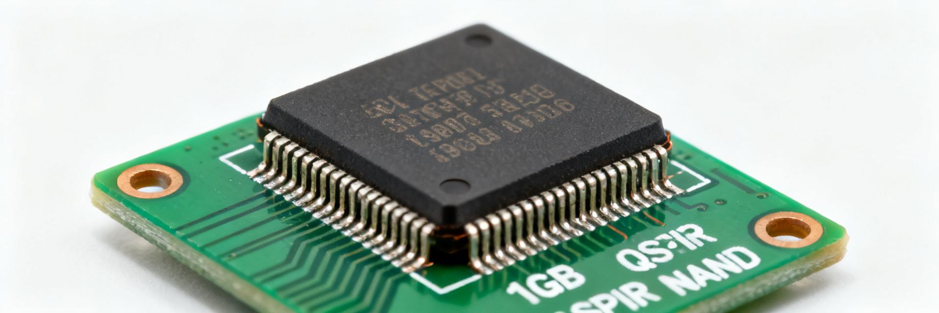
H5AN8G6NDJR-VKC DDR4 Specs & Pinout: Performance Deep Dive
As legacy and embedded platforms continue to rely on DDR4, understanding device-level tradeoffs matters more than ever; this deep dive on the H5AN8G6NDJR-VKC links part-level characteristics to system throughput and validation needs. The article scope covers spec reading, pinout and layout, performance calculations, and an integration checklist to validate designs.
This introduction uses manufacturer datasheet parameters and JEDEC guidance as evidence for assertions about voltage, density and speed. Readers will get practical formulas, PCB layout rules, and a prioritized bring-up checklist aimed at helping engineers translate DDR4 specs into reliable system behavior.
What the H5AN8G6NDJR-VKC Is: Device overview (background)
Density, organization & target applications
Point: The device is an 8 Gb DDR4 component organized to support common x8/x16 data widths, suitable for client and embedded modules. Evidence: The datasheet lists an 8-gigabit density and common organization options. Explanation: Density and organization determine channel width, rank mapping and whether a single device fits a desired module topology.
Package, thermal & supply envelope
Point: The part uses an FBGA package with multiple power and ground balls and requires standard DDR4 rails. Evidence: Manufacturer documentation specifies nominal VDD around 1.2 V and separate VDDQ/I/O domains, plus operation over extended temperature ranges. Explanation: Proper supply routing, decoupling and thermal allowance are essential to avoid timing shifts and training failures.
DDR4 specs: timing, speed grades & electrical parameters (data analysis)
Key timing parameters to read and how to interpret them
| Parameter | Description | Impact |
|---|---|---|
| CL (CAS Latency) | Clock cycles between READ command and data availability | Affects read latency directly |
| tRCD | Row Address to Column Address Delay | Impacts access time to new rows |
| tRP | Row Precharge Time | Time required to close a row before opening another |
| tRAS | Row Active Strobe | Minimum time a row must remain active |
Point: CL, tRCD, tRP, tRAS and tFAW are the primary timing entries engineers use to estimate latency and parallelism. Evidence: Datasheet timing tables and JEDEC definitions map CL and MT/s to absolute latency. Explanation: For example, at 2666 MT/s a CAS latency of 16 yields CAS latency ≈ (CL × 1000) / (MT/s ÷ 2) ≈ 12.0 ns, showing CL and rate together set absolute access time.
Voltage, I/O characteristics and refresh behavior
Point: DDR4 electricals—nominal 1.2 V core, defined I/O swing and on-die termination—drive power budgeting and controller settings. Evidence: The device lists VDD, VDDQ and recommended VREF ranges and tREFI refresh intervals. Explanation: Designers must account for refresh energy (periodic tREFI events) and set VREF/ODT properly to maintain signal integrity and predictable power consumption.
Pinout, ball map & recommended PCB footprint (pinout)
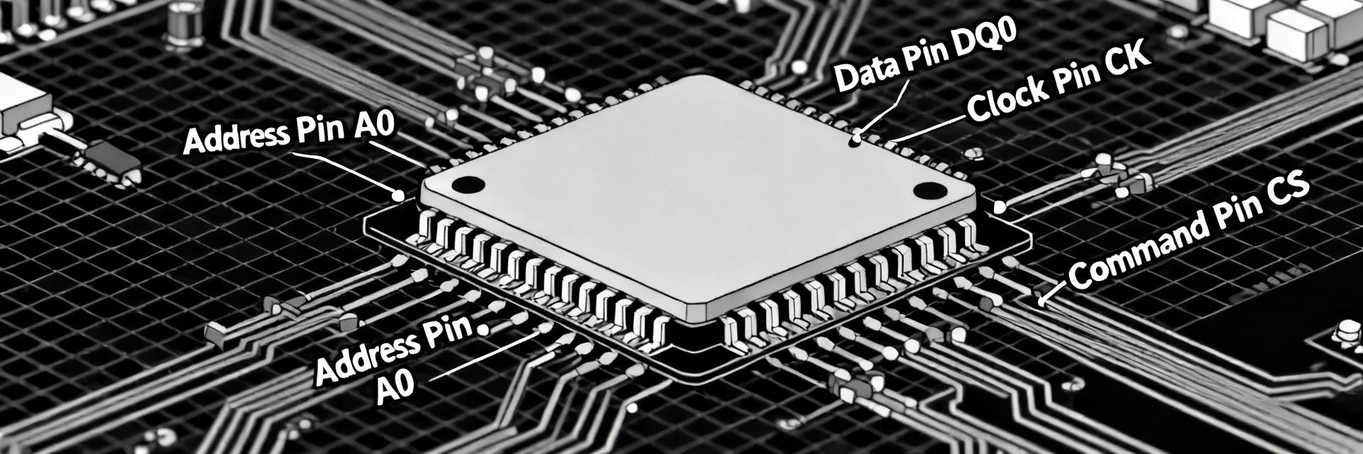
Pin grouping: address/control, DQ, DQS, Vdd/Vss and special pins
Point: Ball maps group command/address, data (DQ), strobes (DQS) and power/ground for predictable routing. Evidence: The ball map shows clusters of Vdd/Vss and distinct lanes for CK/CK# and CA/command. Explanation: Identifying reserved/no-connect balls and common power pins early avoids routing errors and ensures correct decoupling and return-path planning on the PCB.
Layout best practices: routing, decoupling & return paths
Point: Signal integrity requires matched DQ/DQS pairs, controlled impedance, and dense decoupling near power balls. Evidence: Established DDR4 layout practices call for matched-length DQ/DQS within tens of mils and multiple local decouplers per power ball. Explanation: Follow differential routing for strobes, length-match DQ to DQS, place caps within a small loop area, and use solid power planes for low impedance return paths.
Performance deep-dive: bandwidth, latency & real-world throughput (data analysis)
Theoretical bandwidth vs effective throughput
Point: Peak bandwidth is MT/s × bus width ÷ 8; usable throughput is lower due to overhead and ECC. Evidence: At 2666 MT/s a x16 device yields peak per-device bandwidth of 2666 × 16 ÷ 8 ≈ 5.33 GB/s. Explanation: In real systems rank/slot mapping, ECC bits, and refresh windows reduce sustained throughput; for example ECC can consume ~1/9 of raw transfer if an extra chip implements parity/CRC.
Benchmark methodology and board-level factors
Point: Measured results depend heavily on controller timings, training, and board quality. Evidence: Controlled tests use JEDEC timing profiles, fixed refresh settings and read/write patterns to isolate device behavior. Explanation: When benchmarking, compare sustained random-access and burst sequential patterns, log training convergence and watch for thermal or power noise that will depress observed throughput relative to theoretical limits.
Integration & design checklist: controller settings, power sequencing & validation (method guide)
Memory controller configuration & timing training
Point: Correct controller programming and training are mandatory for reliable operation. Evidence: Logs indicating failed training or ODT misconfiguration commonly point to timing or VREF mismatches. Explanation: After bring-up, run read/write pattern tests, verify training status flags, and iterate ODT/VREF and CAS/tRCD/tRP settings until deterministic pass rates are achieved.
Power sequencing, thermal management & reliability testing
Point: Power-up/-down order and thermal headroom affect long-term reliability. Evidence: Recommended sequences show VDD and VDDQ ramp ordering and VREF verification before command enable. Explanation: Implement correct sequencing, monitor junction temps under stress, and perform accelerated burn-in with worst-case patterns to reveal marginal power or signal integrity issues before production.
Use cases, module configurations & troubleshooting checklist (case + action)
Typical module and rank configurations (single-rank, dual-rank, stacked)
Point: The device fits single- or multi-rank module designs; rank choice impacts latency and interleaving. Evidence: Using one or multiple devices per rank changes channel timing and address mapping. Explanation: Single-rank modules simplify controller training, while dual-rank or stacked configurations increase density but require careful timing calibration and possibly reduced top-line frequency.
Troubleshooting: common failures and stepwise diagnostics
Point: Start with power rail checks, then signal integrity captures and training logs to isolate failures to device, board, or controller. Evidence: Typical failure modes show power dropouts, oscilloscopic eye closure, or repeated training retries. Explanation: Collect VRM readings, scope DQ/DQS/CK, capture controller logs, and run targeted memory patterns to narrow root cause before replacing parts.
Key Summary
- The H5AN8G6NDJR-VKC is an 8 Gb DDR4 device; check the manufacturer datasheet for organization and voltage specs to match module and controller choices, as density sets channel width and mapping constraints.
- Read DDR4 specs for CL, tRCD and MT/s to compute absolute latency; practical latency is CL × (cycle period) and 2666 MT/s with CL16 gives roughly 12 ns CAS time.
- Pinout-aware PCB layout—matched DQ/DQS, controlled impedance, close decoupling and correct power sequencing—directly preserves achievable throughput and reduces training failures.
Summary
Recap: the H5AN8G6NDJR-VKC delivers 8 Gb DDR4 density with standard 1.2 V rails and defined timing grades; engineers should use the datasheet for exact DDR4 specs, follow pinout and layout best practices, and validate with controlled benchmarks and a strict integration checklist before production.
FAQ
What are the critical DDR4 specs to verify for H5AN8G6NDJR-VKC?
Verify density, organization, nominal VDD/VDDQ, CL/tRCD/tRP values and supported MT/s from the device datasheet. Also confirm VREF and ODT settings for the target controller. These parameters determine latency, power and whether the part fits the intended module configuration.
How should engineers approach pinout verification for H5AN8G6NDJR-VKC?
Cross-check the ball map to identify Vdd/Vss clusters, DQ/DQS lanes and command/address balls; ensure reserved/no-connect balls are not tied. Validate PCB footprint against recommended land pattern, and place decoupling caps close to power balls to maintain low impedance.
Which validation steps best map DDR4 specs to measured performance?
Use controlled JEDEC-like timing profiles, run sequential and random throughput tests, monitor training logs and thermal conditions, and instrument power rails. Correlate measured bandwidth and latency against theoretical MT/s×width calculations to isolate board-level losses.
What causes common training failures in DDR4 integration?
Training failures often stem from incorrect VREF/ODT settings, poor signal integrity due to unmatched trace lengths, insufficient decoupling causing noise on power rails, or improper power sequencing during startup.