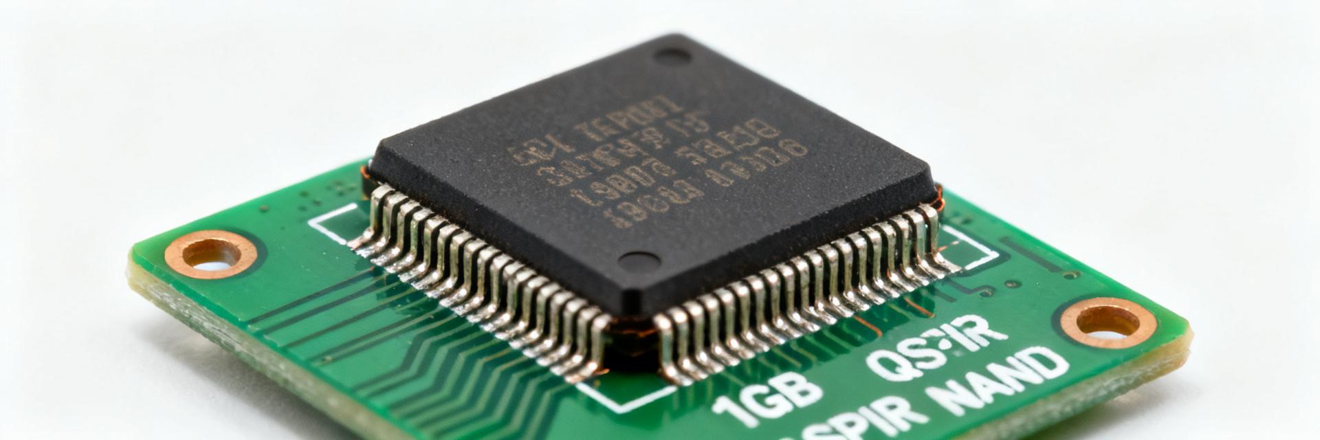
H5ANAG8NCJR-XNC 16Gb DDR4: Complete Technical Report
1 — Background & Product Overview
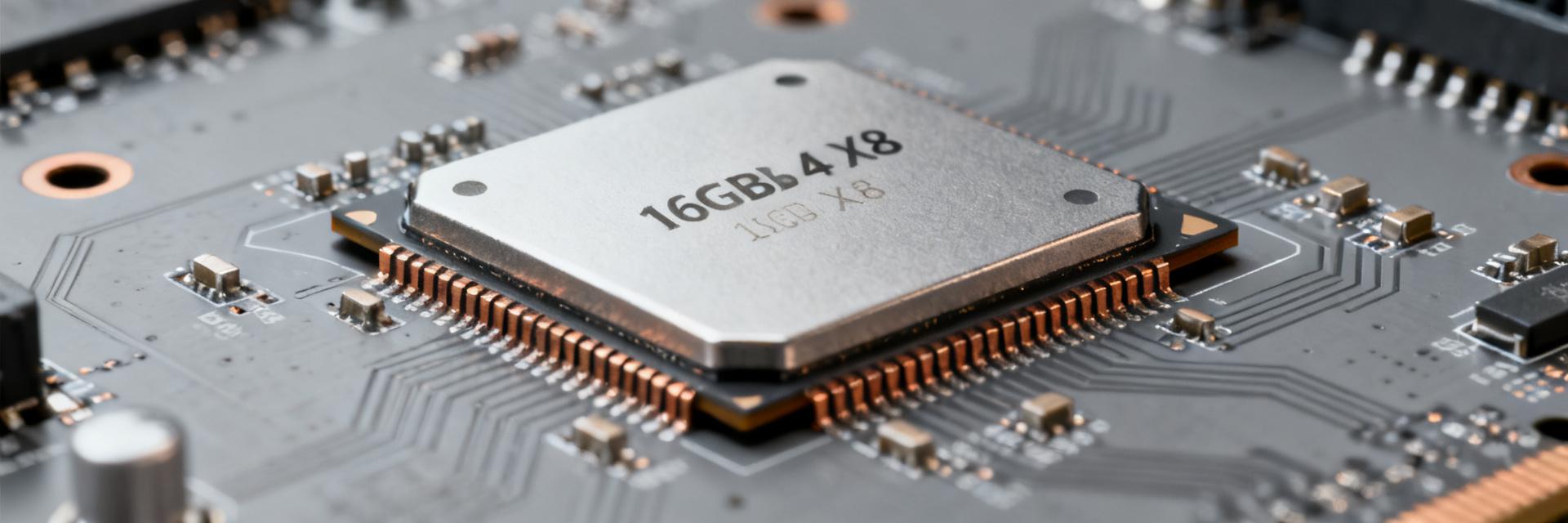
Device Architecture & Logical Organization
The H5ANAG8NCJR-XNC device is a high-density monolithic 16Gb (Gigabit) Double Data Rate 4 (DDR4) SDRAM component structured logically as a 2G x8 array. Internally, the memory array is divided into multiple bank groups to achieve optimal pipelining speeds. Board-level systems treat the chip as a standard 8-bit wide element, allowing designers to assemble flexible rank configurations (e.g., building a 64-bit wide channel with eight parallel x8 chips).
| Organization | Bit-Width | Target Module Configurations |
|---|---|---|
| 2G x8 | x8 | Single-rank 8-chip (8GB), Dual-rank 16-chip (16GB) |
| 4G x4 (Logical Variant) | x4 | High-density multi-rank register-buffered enterprise modules |
Target Applications & Market Context
This 16Gb density device caters heavily to telecommunication equipment linecards, embedded hardware controllers, legacy server upgrade cycles, and fanless industrial computing architectures. Moving to a 16Gb-per-die design directly minimizes board size, reduces trace routing congestion relative to using multiple 8Gb chips, and preserves platform lifecycles without requiring complete SOC upgrades.
2 — Key Electrical Specifications & Package Details
Core Electrical Specs & Timing Parameters
The operating parameters of the device follow standard JEDEC DDR4 guidelines, running on a 1.2V core Vdd line. Operating speed classes scale up to DDR4-3200, enabling robust performance under peak processing configurations. CAS latency profiles typically span from CL14 to CL22 depending on the selective speed-binning of the controller.
| Parameter | Typical Value | Note / Test Condition |
|---|---|---|
| Vdd (Core) | 1.2 V ± 0.06V | Standard supply range per JEDEC specification |
| Data Rate | Up to 3200 MT/s | Dependent on system controller configuration |
| tCL (CAS Latency) | 14–22 cycles | Optimized by firmware training cycle |
| Operating Temp Range | 0°C to 85°C | Extendable to 95°C with double refresh rates |
Package, Pinout & Physical Considerations
Available in a standard FBGA package footprint, the device balances structural stability and routing escape pathways. Hardware layout teams must pay critical attention to target lands, matching trace dimensions to high-density ball matrices, and providing appropriate physical clearances underneath to suppress interference.
3 — Performance Characteristics & Thermal / Signal Integrity
Bandwidth, Latency & Benchmark Expectations
Calculating maximum capabilities, a single x8 device operating at 3200 MT/s yields a peak bandwidth of approximately 3,200 MB/s. Parallel layout designs utilizing a full 64-bit channel configuration achieve a theoretical ceiling of up to 25,600 MB/s. Real-world continuous bandwidth relies heavily on controller logic optimization, queue deepness, and the percentage of continuous sequential memory blocks accessed.
Thermal Profile & Signal Integrity Guidance
Under active read/write cycling, power dissipation ranges upwards of several hundred milliwatts per component. To preserve stable junction temperatures below threshold maximums, PCB designs must integrate continuous ground plane pours and thermal relief vias directly near the device grounding pins. Signal integrity is best maintained through careful routing matching of differential clock traces and proper application of On-Die Termination (ODT) values inside controller profiles.
4 — Integration Guidelines for System Designers
PCB Layout & Routing Best Practices
- Impedance Targets: Design with 50-ohm single-ended and 100-ohm differential trace targets across system layers.
- Length Matching: Match address/command signal lengths to the master system clock trace with sub-picosecond tolerances.
- Layer Transitions: Minimize routing transition vias to prevent localized parasitic inductance.
- Decoupling Matrix: Mount 0.1µF and 4.7µF capacitors as close as structurally feasible to the power entry balls.
Power Delivery Network (PDN) & Controller Calibration
To avoid memory access faults caused by transient voltage spikes, the power delivery network must support rapid current demands with minimal loop impedance. Systems engineers should initially load default, conservative timing margins inside BIOS profiles to secure base-level bootups, and gradually tighten parameters through ODT calibration routines and read/write signal testing sweeps.
5 — Use Cases & Comparative Positioning
Typical System Deployments
The device is widely applied in multi-rank hardware environments where total capacity overrides simple raw clock rates. A standard dual-rank layout using 16 separate chips realizes 32GB of highly structured server RAM. Alternatively, space-restricted industrial computing motherboards can implement single chips directly down on the main motherboard deck for localized processing caches.
Comparison vs. Alternative DDR4 Densities
When stacked against alternative 8Gb solutions, the 16Gb H5ANAG8NCJR-XNC offers double the spatial memory density. This prevents the need to incorporate multi-layered stack layouts on space-constrained mainboards. However, the larger addressing matrix of 16Gb modules requires memory controller firmware and physical BIOS configurations fully capable of interpreting extended address layouts.
6 — Reliability, Qualification & Procurement Recommendations
Qualification Checklist & Thermal Stress Validation
Before launching hardware into production environments, teams must run comprehensive DDR4 stress validation sequences. Testing procedures must cover extreme heat/cold thermal cycles, High-Temperature Operating Lifetime (HTOL) testing, and continuous ECC diagnostic error logging on target devices to detect early failure profiles.
Sourcing, Lifecycle and Obsolescence Safeguards
For sustainable mass production cycles, ensure components are sourced exclusively from authorized distributors with full trace certificate documentation. To avoid potential project stoppages from sudden component lifecycle changes, physical layouts should ideally remain pin-compatible with multi-sourced alternative standard DDR4 16Gb FBGA packages.
Summary: Successful execution using the H5ANAG8NCJR-XNC 16Gb DDR4 component requires confirming fundamental electrical specs, adhering strictly to target routing impedances, providing optimal active heat paths, and setting up systematic sourcing policies.