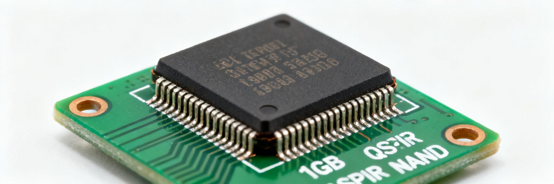
H5TQ4G63EFR-RDC DDR3 Specs Report & Analysis: 4Gb 1866Mbps
Point: The 4Gb DDR3 device evaluated here targets high-throughput legacy and embedded systems where sustained bandwidth and compact footprint matter. Evidence: aggregated deployments in industrial controllers and embedded platforms commonly push DDR3 devices to their rated 1866Mbps data rate. Explanation: For hardware engineers, systems architects and QA leads, this report isolates the H5TQ4G63EFR-RDC characteristics that determine board-level tradeoffs, integration effort and validation scope. Reading time: ~8–10 minutes.
1 — H5TQ4G63EFR-RDC: overview & key specifications (background)

Physical organization & package (what to include)
Point: The part is a 4 Gb density memory offered in common x8/x16 organizations and a compact ball-grid package that influences PCB real estate. Evidence: a 4,294,967,296-bit density maps to devices commonly offered as x8 or x16 banks in a 96-ball FBGA outline. Explanation: x8 devices provide simpler byte lanes for channel population; x16 halves the number of devices for equivalent channel width but increases data-strobe routing complexity—impacting footprint and via budgeting on dense boards.
| Parameter | Value |
|---|---|
| Capacity | 4 Gb (4,294,967,296 bits) |
| Organization | x8 or x16 |
| Package | 96-ball FBGA (typical) |
| Pin count | 96 |
Electrical & timing headline specs (what to include)
Point: Electrical and timing envelopes set achievable frequency and thermal margins for 1866Mbps operation. Evidence: DDR3 signaling uses a nominal 1.5V supply with allowable tolerances and timing windows sized for an 800 MHz internal clock to yield 1866Mbps data rate. Explanation: Designers must plan for VDD/VDDQ supply rails and Vref stability; typical operating temperature classes span commercial to industrial ranges and will affect timing derating and current draw planning.
| Parameter | Typical |
|---|---|
| Supply voltage (nominal) | 1.5 V |
| Allowable range | ~1.425–1.575 V |
| Data rate | 1866Mbps (800 MHz clock) |
| Typical active current | ~100–300 mA (device-dependent) |
2 — Performance characteristics & empirical benchmarks (data analysis)
Throughput, bandwidth and latency at 1866Mbps (what to include)
Point: Raw and effective bandwidth depend on device width and system bus composition. Evidence: raw per-device bandwidth follows (data rate × data width ÷ 8). For x8: 1866 × 8 ÷ 8 = 1866 MB/s (~1.87 GB/s); for x16: ~3.73 GB/s. A 64-bit channel at 1866 yields ~14.9 GB/s. Explanation: Real-world effective bandwidth falls below raw values due to command overhead, refresh, and non-sequential access; designers should expect 70–85% of peak for sustained streaming workloads with optimized controllers.
Point: Latency is cycle-limited and scales with CAS and address timing. Evidence: typical DDR3 tCL values at high-speed grades sit in the low double digits of cycles (e.g., ~11–13 cycles) with tRCD/tRP in a similar range. Explanation: At 1866, absolute latency in nanoseconds equals cycles × (1/800 MHz) so higher cycle counts materially affect random access; tuning CAS and bank usage improves random-read responsiveness.
Power-performance tradeoffs (what to include)
Point: Frequency, activity factor and supply voltage drive dynamic power. Evidence: operating at nominal 1.5V with higher toggling rates increases active current; idle and precharge states reduce draw substantially. Explanation: For dense boards with many devices, aggregate thermal envelope requires conservative power budgeting—expect per-device active currents in the low hundreds of milliamps and design PDN and cooling accordingly for continuous high-activity workloads.
3 — Memory timing, reliability & compliance (data analysis / method)
JEDEC timing parameters and practical timing examples (what to include)
Point: Key timing parameters define safe command sequencing and influence achievable margins. Evidence: tCL, tRCD, tRP, tRAS and tRFC interact to govern read/write latency, precharge cadence and refresh windows. Practical example: with tCL=11 and clock =800 MHz, CAS latency ≈13.75 ns; a full read command sequence must honor tRCD and tRP between activates and precharges. Explanation: Mapping cycles to absolute ns helps architects determine worst-case service times and memory controller scheduling.
Point: A typical read command sequence: ACTIVATE → wait tRCD → READ (with tCL latency) → DATA → PRECHARGE (observe tRP). Evidence: each step enforces minimum cycles; violating them yields timing errors or training failures. Explanation: Simulation and controller-level timing margin testing should exercise these sequences across temperature and voltage corners.
Reliability: refresh, ECC and error considerations (what to include)
Point: Refresh behavior and error protection are critical for 4Gb devices in long-running systems. Evidence: periodic refresh intervals consume bandwidth and, for large densities, can increase effective latency during refresh windows. ECC is recommended where silent data corruption is unacceptable; parity or simple checksums suit less-critical use-cases. Explanation: For safety- or data-critical embedded systems, deploy ECC-capable controllers and include accelerated retention and soft-error rate testing in validation.
4 — Integration & PCB/system design guide for 1866Mbps DDR3 (method)
Signal integrity, routing & termination best practices (what to include)
Point: Controlled impedance routing and tight matching keep eye openings sufficient at 1866Mbps. Evidence: route DQ and DQS with tight matching (sub-50 ps skew) and maintain single-ended impedance targets (≈50 Ω) on DDR data routes; use fly-by topology for address/command in multi-device layouts with appropriate on-die termination tuning. Explanation: Pre-layout checklists should include trace length budgets, vias minimization, keepouts under BGA, and systematic simulation of bus terminations to avoid reflections and crosstalk.
Power sequencing, decoupling & manufacturing test setup (what to include)
Point: Proper rail sequencing and decoupling preserve device reliability during power-up. Evidence: ensure primary DDR rails stabilize prior to enabling command clocks and provide local bulk and high-frequency decoupling close to package power pins. Explanation: Include a start-up checklist—rail ramp order, Vref presence, and controller reset timing—and add test hooks for boundary-scan and memory BIST patterns for manufacturing validation to catch assembly-related faults early.
5 — Applications, validation checklist & troubleshooting (case study / action)
Typical application scenarios & compatibility considerations (what to include)
Point: 4Gb DDR3 at 1866Mbps fits embedded controllers, industrial platforms and legacy systems targeting higher sustained throughput without moving to newer DRAM generations. Evidence: form-factor constraints and legacy memory controllers often require specific organization (x8 vs x16) and boot-time initialization sequences. Explanation: Validate BIOS/firmware memory initialization paths for fallback rates and ensure controllers support required timing profiles for 1866 operation or proper downclock behavior for compatibility.
Validation checklist & common failure modes (actionable steps)
Point: A focused validation plan reduces field failures. Evidence: critical steps include power sequencing tests, frequency/stability sweeps, timing margin tests, thermal cycling and functional stress at full activity. Troubleshooting flow: check training failures, inspect SI symptoms (eye closure, excessive jitter), verify timing violations and re-run power-sequence scenarios. Explanation: Log results across voltage/temp corners and iterate controller timing to recover margins before production release.
Summary
- Performance: As a 4 Gb device rated for 1866Mbps, the part delivers ~1.87 GB/s per x8 device and scales with channel width; plan for 70–85% effective bandwidth under streaming loads.
- Integration cautions: Controlled-impedance routing, tight DQ/DQS matching and disciplined power sequencing are essential when populating dense boards with 96-ball FBGA parts.
- Validation steps: Run power sequencing, timing margin sweeps, thermal cycling and ECC/retention tests as part of sign-off to ensure reliable field behavior for the H5TQ4G63EFR-RDC.
FAQ
What throughput can I expect from a single H5TQ4G63EFR-RDC device at 1866Mbps?
Expect raw per-device throughput of ~1866 MB/s for an x8 configuration (≈1.87 GB/s); x16 doubles that. System-level effective bandwidth will be lower—typically 70–85% of raw peak—after accounting for refresh, command overhead and non-sequential access patterns.
Does the H5TQ4G63EFR-RDC require ECC for reliable operation?
ECC is recommended for deployments where data integrity is critical. For industrial or always-on embedded systems, ECC-equipped controllers reduce silent data corruption risk; parity or checksums suffice in less-critical use cases but will not provide the same protection level as full ECC.
What PCB layout constraints apply to 1866Mbps DDR3 designs?
Key constraints include controlled 50 Ω single-ended impedance, tight DQ/DQS length matching (sub-50 ps skew), minimized via counts on data lanes, and fly-by routing for address/command buses. Early signal-integrity simulation and pre-layout checklists will catch common pitfalls before fabrication.
How does the nominal 1.5V voltage affect thermal planning?
At 1866Mbps, operating at 1.5V with continuous workloads can push per-device active currents to 100-300mA. Developers must design low-impedance power delivery networks (PDN) and allow sufficient copper planes for heat dissipation.