NL0333DCAE1S-ES Datasheet Deep Dive: Specs & Pinout
Low-voltage, rail-to-rail single-ended amplifiers are central to modern portable and sensor systems where headroom and power budget are constrained. This article delivers a practical, component-level walkthrough of the NL0333DCAE1S-ES datasheet so engineers can evaluate typical specs, interpret the pinout, and integrate the part into prototypes with confidence.
(1) Component Overview & Key Use Cases
The NL0333DCAE1S-ES is a low-voltage, rail-to-rail input/output operational amplifier suited for single-supply portable systems. Typical roles include sensor front-ends, battery-powered instrumentation, and compact audio preamps where headroom and quiescent current are critical.
| Parameter | Typical Datasheet Value |
|---|---|
| Supply Voltage Range | 1.8 V – 5.5 V (Single Supply) |
| Input Common-Mode Range | Rail-to-Rail (VSS-0.1 to VDD+0.1) |
| Output Swing | Within 50mV of Rails (Light Load) |
| Quiescent Current | Low µA to sub-mA class |
| Package Type | SOT-23-5 |
(2) Pinout & Packaging Details
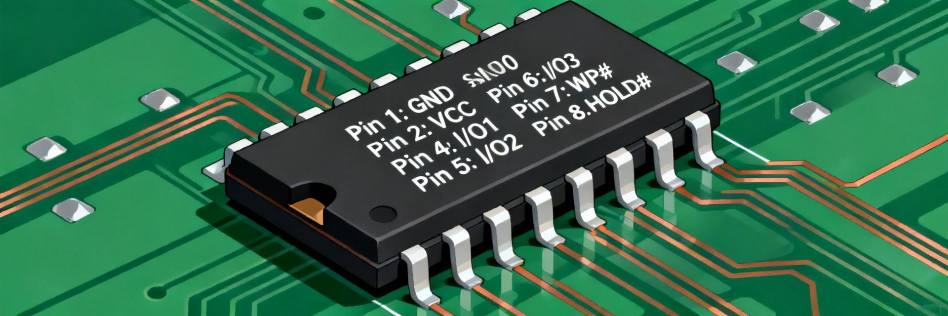
The standard SOT-23-5 configuration for the NL0333DCAE1S-ES provides a compact footprint. For PCB design, ensure the decoupling capacitor (0.1 µF) is placed within 2mm of Pin 5 (V+). Footprint accuracy is essential; follow standard IPC-7351 patterns for SOT-23-5 to ensure thermal and mechanical reliability.
(3) Electrical Specifications Deep Dive
DC characteristics: power, offsets, bias
DC specs govern accuracy and battery drain. Input offset voltage (Vos) and drift directly affect ADC front-end accuracy. For example, a 100 µV offset at a 2.5 V full-scale input produces significant ppm error. Always check the NL0333DCAE1S-ES datasheet for the maximum quiescent current to calculate the worst-case battery life.
AC characteristics: bandwidth, slew rate, noise
AC parameters determine dynamic response. Slew rate indicates how the device handles fast edges, while input-referred noise determines SNR. For sensor sampling, prioritize bandwidth above the anti-aliasing corner to avoid signal distortion.
(4) Typical Application Circuits & Design Guidelines
Common circuits include unity-gain buffers and non-inverting amplifiers. Layout drives performance: route input traces short and shielded, and use ground pours. For capacitive loads, add a series output resistor (10–47 Ω) to prevent oscillation and ensure phase margin stability.
(5) Troubleshooting & Integration Checklist
- Verify Pinout: Cross-check physical Pin 1 marking with the CAD library.
- DC Bias: Confirm the input signal stays within the common-mode range (VSS to VDD).
- Decoupling: Use low-ESR ceramic capacitors close to the supply pins.
- Thermal: Check junction temperature in enclosed or high-ambient environments.
Key Summary
- Pinout clarity: Verify SOT-23-5 pin mapping and any EN or NC pins before PCB release.
- Critical specs: Confirm supply range (1.8-5.5V), input common-mode, and offset for ADC accuracy.
- Layout & testing: Place decoupling caps close to VCC and add output series resistance for capacitive loads.
Frequently Asked Questions
How do I confirm the NL0333DCAE1S-ES pinout on my PCB?
Which electrical characteristic most affects ADC front-end accuracy?
What quick bench tests reproduce datasheet conditions?
How to handle capacitive loads with NL0333DCAE1S-ES?
End of Technical Analysis for NL0333DCAE1S-ES. For production-grade designs, always refer to the latest revision of the official manufacturer datasheet.