H5CG48AGBDX018N DDR5-5600 : Rapport de performances et de spécifications
Executive Summary: This report evaluates the H5CG48AGBDX018N DDR5-5600 part with a data-first focus to set realistic expectations for system designers and procurement teams. Specification references and benchmark-oriented test plans drive the analysis. Readers will get practical guidance on throughput, integration checkpoints, validation steps, and procurement considerations for balanced client and server use cases.
The device is a 16Gb DRAM die intended for high-density module assembly; its FCBGA packaging and 1.1V operation influence PDN (Power Delivery Network) and thermal choices. Datasheet tables (electrical, timing, package) are the basis for recommended PDN sizing and signal integrity (SI) checks. The remainder of this report translates those tables into actionable board- and system-level tasks.
Background: What “DDR5-5600” and H5CG48AGBDX018N mean
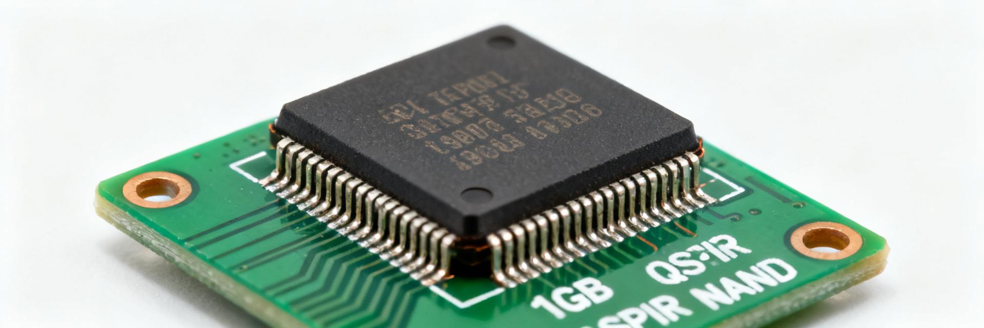
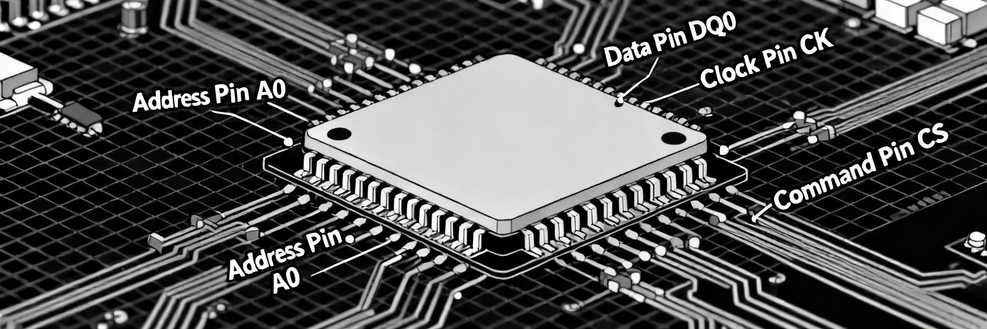
For context, see the core physical block orientation below representing standard module-level physical placement and signal flows.
Definition & JEDEC context
DDR5-5600 denotes a speed grade of 5600 MT/s under the DDR5 JEDEC framework. JEDEC speed bins define MT/s and set baseline operating envelopes; effective data rate is MT/s multiplied by channel width to estimate raw bandwidth. For designers, interpreting MT/s, transfers per cycle, and channel width is the first step to convert part speed into system-level throughput expectations.
Part identity & key package/organization facts
The H5CG48AGBDX018N is a 16Gb component with 2Gx8 organization in FCBGA packaging and a 1.1V nominal supply. Density and x8 organization determine module rank and lane mapping, while FCBGA ballout affects routing and thermal footprint. These attributes guide choices for DIMM rank population, channel balancing, and module assembly in multi-rank configurations.
Architecture & Key Electrical/Physical Specs Deep-Dive
Electrical characteristics and power behavior
Nominal 1.1V operation and DDR5 power-management features reduce operating current but shift PDN design constraints. IDD class measurements (active, standby, refresh) in datasheets inform decoupling and regulator headroom. Engineers should size 1.1V rails with margin for peak IDD spikes during training and use staged decoupling to control switching noise and maintain signal integrity.
Physical/package and timing parameters that matter
Package attributes (ball pitch, BGA height) plus timing values (CL, tRCD, tRP) directly affect thermal, mechanical, and latency budgets. BGA thermal footprint and ballout constrain copper pours and via placement; timing numbers convert MT/s into absolute nanosecond latency. High MT/s reduces cycles per transfer but absolute ns latency can rise; board routing and heat dissipation must account for dense BGA arrays and higher switching activity.
| Parameter Type | Specification Key Metric | Design Target Value | System-Level Impact |
|---|---|---|---|
| Memory Density | 16Gb (Gigabit) | 2Gx8 Configuration | Dictates physical address mapping & ranks |
| Supply Voltage | VDD / VDDQ Nominal | 1.1V Operation | Improves thermal margins; shifts transient limits |
| Target Timing | CL-tRCD-tRP Bins | Speed Bin DDR5-5600 | Calculates exact cycles vs absolute ns latency |
| Packaging | FCBGA Ball Array | Fine Pitch Array | Governs routing layers & under-die decoupling |
Performance & Benchmarks Analysis (data-oriented)
Synthetic and real-world test matrix
A reproducible test matrix must combine microbenchmarks and application-level workloads to reveal bandwidth and latency behavior. Use STREAM for sustained bandwidth, dedicated latency microbenchmarks for ns timing, and application tests (database TPS, ML memory-bound kernels, graphics frame-buffer stress). Control variables include module rank/population, channel count, CAS/timing profiles, and training results to ensure apples-to-apples comparisons at DDR5-5600.
Interpreting results: throughput vs latency trade-offs
Higher MT/s delivers clear bandwidth advantages for memory-bound workloads, while latency-sensitive tasks may see modest or no gain. Bandwidth scales roughly with MT/s times bus width; absolute ns latency depends on CL and cycle period. Expect measurable improvements in streaming and large working set applications; tight-loop, low-RPC workloads will depend more on CAS and training-optimized timings than raw MT/s alone.
Integration & System Design Guide
Board-level, SI and power-delivery considerations
Signal integrity and PDN design are critical for reliable 5600 MT/s operation with 16Gb parts. Match channel lengths, manage stub minimization, implement proper termination, and provision robust decoupling on the 1.1V rail. Designers should allocate controlled impedance traces, differential pair matching where applicable, dedicated VRM headroom for IDD peaks, and targeted bulk/MLCC placement near the BGA for transient suppression.
Firmware/BIOS and validation priorities
Memory training and SPD provisioning are central to bringing up DDR5 modules with complex rank and timing interactions. Training sequences exercise DQ timing, Vref calibration and CA timing; SPD (or firmware descriptors) must reflect the 2Gx8 mapping and supported timing bins. Validation should follow a phased flow: basic boot, training validation, stress burn-in, and ongoing error-rate monitoring to ensure stable timing under thermal and voltage excursions.
Comparative Analysis & Selection Criteria
Trade-offs vs other DDR5 speed grades and densities
DDR5-5600 16Gb parts represent a balance between bandwidth, power and cost versus lower or higher speed bins. Lower speed grades reduce SI and PDN stress and often lower BOM cost; higher bins increase peak bandwidth but raise validation and thermal needs. Choose DDR5-5600 for balanced cost/performance in bandwidth-sensitive but budget-constrained platforms; prefer higher grades only when sustained bandwidth is the dominant system bottleneck.
Cost, supply and longevity considerations for procurement
Procurement decisions hinge on lead time, qualification effort and long-term lifecycle support for a chosen density/speed. Higher-speed/high-density parts can require extended qualification runs and additional sample quantities for margin testing. Buyers should request qualification samples, schedule qualification cycles into project timelines, and factor potential premium pricing and inventory lead times into BOM risk assessments.
Deployment Checklist & Actionable Recommendations
Pre-deployment validation checklist
A concise, stepwise validation checklist reduces integration surprises. Define pass/fail thresholds per step (training success, no correctable errors during 24–72 hour burn-in, stable Vref under load) and gate mass deployment on meeting these criteria:
- Datasheet Cross-Check: Verify footprint match and pinout layout against production board files.
- PDN Verification: Scope 1.1V rail close to the BGA pads to capture transient droop during peak write commands.
- SI Verification: Check waveform eye margin on DQ/DQS lines under extreme low/high voltage sweeps.
- Firmware Validation: Confirm stable boot across variable ambient conditions with active timing calibration.
- Thermal Stressing: Validate target airflow speed and ambient envelope at continuous maximum bandwidth.
Purchase, qualification and lifecycle monitoring recommendations
Authentic sourcing and continuous monitoring preserve long-term platform reliability. Qualification plans should cover sample acceptance tests, in-field telemetry for corrected/uncorrected error rates, and firmware regression checks after updates. Maintain traceability for parts, run periodic requalification after major platform changes, and track margin metrics to detect performance regressions early.
Summary
The H5CG48AGBDX018N operating at DDR5-5600 is a 16Gb, 2Gx8, 1.1V-rated device optimized for balanced bandwidth and power. Datasheet-derived attributes and benchmark-driven validation steps show where system gains are realized. Prioritize PDN and SI work, follow the prescribed test matrix, and use the procurement checklist to qualify parts before large-scale deployment.
Key Summary
- DDR5-5600 provides measurable bandwidth lifts for memory-bound workloads; validate with STREAM and application-level tests to quantify gains per workload.
- The 16Gb 2Gx8 FCBGA device requires deliberate PDN, decoupling and SI practices; size 1.1V rails for IDD spikes and ensure thermal paths for dense BGAs.
- Follow a staged validation plan: bring-up, training validation, extended stress burn-in, and continuous error monitoring before procurement scale-up.
Frequently Asked Questions
How should engineers validate H5CG48AGBDX018N memory timing at DDR5-5600?
Validation should combine training observation and targeted timing sweeps. Run the platform training, capture Vref and CA training logs, then perform CAS and tRCD/tRP sweeps under controlled thermal conditions. Correlate successful training states with the absence of correctable errors during extended stress to identify optimal production timings.
What PDN and cooling practices are recommended for DDR5-5600 16Gb parts?
Strong decoupling and deliberate thermal planning are essential. Place MLCC arrays close to the BGA, provide adequate VRM headroom for transient IDD peaks, and ensure airflow or conductive cooling for dense module assemblies. These measures minimize voltage droop, reduce thermal throttling risk, and keep training stable at high MT/s.
What procurement steps reduce integration risk for DDR5-5600 components?
Structured qualification reduces downstream surprises. Require sample units for platform qualification, specify acceptance test criteria, and plan for lifecycle tracking and requalification after major firmware or platform changes. This approach shortens time-to-reliable-deployment and protects BOM integrity during ramp.
How does the 16Gb 2Gx8 organization affect module rank and lane mapping?
The 2Gx8 configuration means that 8 components must be combined per channel to form a single 64-bit wide rank (or 10 components for ECC). This layout requires careful routing of control and address signals to balance physical line lengths, minimize crosstalk, and ensure synchronous data transfer across the physical lanes under DDR5 timing constraints.