W25N01KVZEIR 规格概览:紧凑技术数据
The W25N01KVZEIR is a compact 1 Gbit QSPI NAND device targeted where board space, low power and fast quad I/O boot or storage matter. This tight, actionable specs snapshot presents core specs, electrical/timing highlights, integration guidance and a practical evaluation checklist so engineers can quickly judge fit for boot, firmware store or small filesystem use. The focus here is on clear, data-driven specs and integration notes engineers can act on immediately.
1 — Quick Product Snapshot (background)
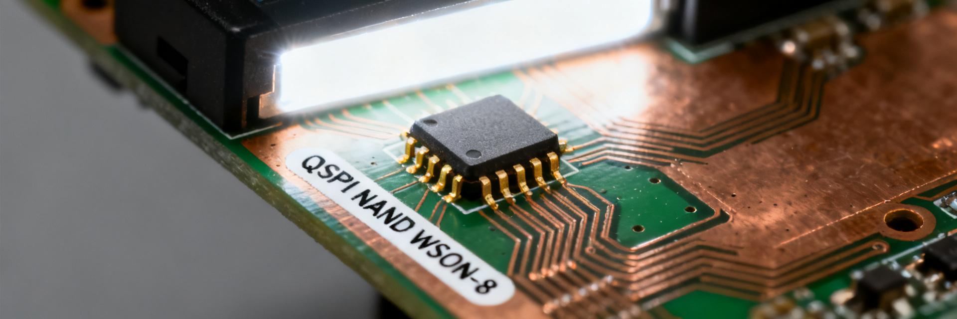
1.1 — At-a-glance specs
| Parameter | Specification Details |
|---|---|
| Part number | W25N01KVZEIR |
| Memory density | 1 Gbit (SLC mode logical organization) |
| Interface | QSPI / Dual / Quad I/O |
| Supply voltage | 2.7 — 3.6 V |
| Package | WSON-8, ~8 × 6 mm |
| Operating temperature | -40 °C to +85 °C |
| Typical active / standby current | Read active ≈ 25–35 mA (typ), Standby ≲ 100 μA (typ) |
| Basic timing | Max clock (QSPI quad) up to ~104 MHz; page program and block erase times device-dependent — see datasheet |
1.2 — Why this snapshot matters
- Density vs. endurance: 1Gbit SLC-style organization gives a compact footprint for code and staging areas where write cycles are moderate.
- Footprint and power: WSON-8 saves board area; low-voltage operation supports battery-powered endpoints and reduced BOM cost.
- Interface speed: QSPI quad I/O reduces boot time versus single-bit serial and simplifies MCU connections with fewer pins than parallel NAND.
2 — Electrical & Timing Details (data analysis)
2.1 — Power, voltage and current characteristics
Operating VCC is specified at 2.7–3.6 V with the I/O domain compatible across typical MCU voltage levels within that range. Designers should confirm recommended VCC decoupling near the device and follow power sequencing notes in the official datasheet (referenced revision). Typical read active current is in the tens of milliamps range; standby currents are in the microamp-to-sub-100-μA range — differentiate typical vs. max values when budgeting system power.
2.2 — Performance & timing (read/program/erase)
QSPI quad clock support typically runs up to roughly 104 MHz for higher-throughput reads; raw read latency and page program/erase times depend on command mode and on-chip operations. On-chip ECC handles bit errors transparently for the host in many modes — verify whether the device reports corrected/uncorrectable counts and how ECC affects usable payload per page. Include timing margin for high-temperature or low-voltage operation and validate worst-case program/erase latencies during system bring-up.
3 — Physical & Integration Considerations (methods / guide)
3.1 — Package, footprint and PCB layout tips
For the WSON-8 ~8×6 mm package, handle the exposed pad per the mechanical recommendation: include a thermal/ground pad with solder mask relief and a recommended land pattern to avoid tombstoning. Place the primary decoupling capacitor within 1–2 mm of VCC pins, route shortest traces for CLK and CMD, and avoid runs under thermal pad splits. Use paste stencil recommendations from the mechanical drawing and confirm MSL and reflow profile during assembly qualification.
3.2 — Signal/interface integration
Pin mapping typically includes CMD, CLK, IO0–IO3, CE and WP/HOLD equivalents; treat high-speed quad lines as matched impedance traces where practical and keep stubs minimal. Use weak pull-ups or pull-downs per the datasheet recommendations for reset/hold pins, and add series resistors (22–47 Ω) on CLK/IO lines to damp reflections if board length warrants. Provide accessible test points and probe access for validating quad reads and toggling CE during debug.
4 — Typical Use Cases & Design Trade-offs (case)
4.1 — Example application scenarios
- Boot/firmware storage for microcontrollers: compact 1Gbit QSPI NAND reduces board area and supports fast quad I/O boot loaders.
- IoT endpoint filesystem: small filesystem or OTA staging area benefits from SLC-like reliability and low pin count.
- Secure boot store or image staging: adequate density for multiple images and low-power retention during sleep modes.
4.2 — Alternatives & selection trade-offs
Selection trade-offs center on endurance vs. density and execution model: parallel NAND offers higher throughput and lower command overhead at the cost of pins; NOR supports execute-in-place but lower density per package. For constrained boards, QSPI NAND like this part balances density, pin count and cost — confirm endurance, ECC coverage and write latency against target application requirements.
5 — Evaluation & Deployment Checklist (action)
5.1 — Pre-procurement checklist
- Verify exact part marking and datasheet revision, confirm moisture sensitivity level (MSL) and reel/tube packaging for assembly.
- Order evaluation samples and a small number of production reels for qualification; request mechanical drawing and recommended land pattern.
- Confirm lifecycle notes and obsolescence guidance in vendor documentation before committing to production BOM.
5.2 — Firmware, ECC and test-plan tips
Enable and validate on-chip ECC reporting, implement wear-leveling or bad-block management in firmware where required, and define factory programming flows for boot images. Plan test cases that include sustained read throughput, measured program/erase timing, retention checks and power-fail recovery. Temperature sweep tests across -40 °C to +85 °C will reveal timing margin and retention shifts that matter in field deployment.
Summary
The W25N01KVZEIR presents a compact 1 Gbit QSPI NAND option that balances footprint, low-voltage operation and quad I/O performance for boot and small storage roles. Key evaluation points are exact electrical and timing figures from the official datasheet, cautious PCB layout for the WSON-8 package, and a firmware plan that leverages on-chip ECC and manages wear. Engineers should consult the official datasheet revision referenced during selection for final numeric values and programming guidance.
Key Summary
- Compact 1Gbit QSPI NAND suitable for boot and small filesystem roles; verify on-chip ECC and endurance before deployment.
- Electrical essentials: VCC 2.7–3.6 V, WSON-8 package, -40 °C to +85 °C operating range and QSPI quad clock up to ~104 MHz.
- Layout checklist: exposed pad handling, close decoupling, short CLK/IO traces, and series damping resistors for signal integrity.
- Evaluation checklist: confirm datasheet revision, MSL, sample quantities, firmware ECC validation, and power-fail test cases.
Frequently Asked Questions
What are the key specs engineers should validate for W25N01KVZEIR?
Engineers should validate supply voltage range, exact active and standby currents, maximum supported QSPI clock, page/program/erase latencies and on-chip ECC behavior as listed in the official datasheet. Confirm package land pattern and moisture sensitivity for assembly and adjust timing margins for worst-case temperature and voltage.
How should firmware handle ECC and bad-blocks for W25N01KVZEIR?
Firmware should read ECC status after operations, implement bad-block management and wear-leveling if multiple writes are expected, and provide fallback for uncorrectable errors. Use the device's ECC reporting to log corrected/uncorrectable counts and include factory programming steps that mark known bad blocks.
What PCB layout practices are recommended for WSON-8 packages like W25N01KVZEIR?
Follow the recommended land pattern, include a properly sized thermal/ground pad with via stitching if specified, place the primary decoupling capacitor within 1–2 mm of VCC, route CLK and CMD as short controlled-impedance traces where practical, and provide accessible test points for high-speed signal validation.
What are the main design trade-offs when selecting QSPI NAND over parallel NAND or NOR Flash?
QSPI NAND balances pin efficiency and footprint size against raw performance. Parallel NAND offers higher throughput but requires substantially more GPIO pins, while NOR Flash supports direct Execute-in-Place (XiP) but is considerably more expensive at high densities such as 1 Gbit.