H5AN8G8NDJR-XNC DDR4データシート:完全仕様およびピン配置
The H5AN8G8NDJR-XNC is an 8‑Gbit DDR4 SDRAM organized as 1G x 8, supporting speed grades up to DDR4‑3200 (3200 MT/s) with a nominal VDD of 1.2 V and an operating window typically 1.14–1.26 V. These numeric anchors explain why this small‑footprint FBGA device suits dense mobile and compact system memory subsystems.
Measured characteristics such as 8 Gb density, x8 organization and low‑voltage 1.2 V operation make this part relevant where power, area and throughput tradeoffs matter; designers will treat this datasheet entry as the basis for power budgeting, routing and timing programming during bring‑up.
Product overview & background — H5AN8G8NDJR-XNC

Product summary and intended applications
Point: The device provides an 8‑Gbit single‑chip capacity in a 1G x 8 organization for mainstream DDR4 roles. Evidence: Density = 8 Gb, organization = 1G x 8, speed window up to 3200 MT/s. Explanation: This combination targets compact client, mobile and embedded controller memory where channel width and per‑chip interleaving define module capacity.
Mechanical package & ordering form factor
Point: The device is supplied in an FBGA small‑footprint package with a high ball‑count for DDR4 signal routing. Evidence: Typical FBGA ball‑map and short nominal dimensions reduce PCB area; shipping formats include trays and tape‑and‑reel. Explanation: Designers should request the ball map/outline drawing for precise courtyard and pick‑and‑place programming and respect moisture sensitivity during reflow.
Electrical characteristics & power (data analysis)
DC electrical specs and power rails
Point: Power budgeting centers on VDD and I/O domains with VREF requirements for stable termination. Evidence: Nominal VDD = 1.2 V with operating window ≈1.14–1.26 V; I/O domain follows VDDQ conventions and requires VREF for DQ termination. Explanation: Refer to the full DDR4 datasheet for complete IDD tables; system designers must size regulators and decoupling to meet active and self‑refresh currents.
| Parameter | Typical | Notes |
|---|---|---|
| VDD | 1.2 V | Operating 1.14–1.26 V |
| IDD Active | Varies by speed grade | See DDR4 datasheet for grade table |
| IDD Self‑Refresh | Low μA–mA range | Important for low‑power designs |
| VREF | VDD/2 | Reference for DQ termination |
Thermal and reliability constraints
Point: Thermal derating and handling are critical for FBGA DDR4 reliability. Evidence: Typical operating temperature ranges and MTBF guidance are provided in the device technical note; elevated junction temperatures reduce retention and lifetime. Explanation: Implement thermal vias under the FBGA, split power planes, and monitor hotspot temperatures during stress testing to prevent long‑term degradation.
Timing and performance parameters (data analysis)
Core timing table — tCK, CL, tRCD, tRP, tRAS, tRC
Point: Timing grade lines map CAS latency and cycle time to MT/s and controller settings. Evidence: For example, a 2666 MT/s grade typically uses tCK ≈0.75 ns and CL values that scale with frequency; 3200 MT/s reduces tCK accordingly. Explanation: Memory controllers must program CAS, tRCD and tRP consistent with the chosen speed grade; wrong settings lead to training failures or data corruption.
Throughput, burst behavior and benchmark implications
Point: Prefetch and burst length determine effective instantaneous bandwidth. Evidence: DDR4 uses an 8n prefetch and bursts that align with DQS strobes; at 3200 MT/s an x8 device yields peak per‑lane throughput proportionate to transfer rate. Explanation: Effective sustained bandwidth depends on controller scheduling, bus efficiency and refresh interruptions; calculate expected throughput by multiplying MT/s × data width × active lanes.
Pinout & package ball map (pinout) — H5AN8G8NDJR-XNC
Complete pin/ball map breakdown
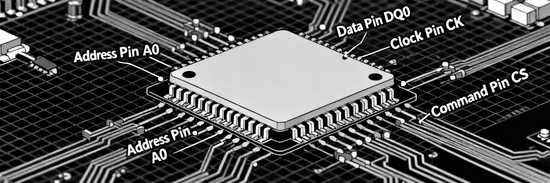
Point: Grouping balls by function simplifies routing and signal integrity planning. Evidence: Typical groups include address/command (A, BA, CSn), clock (CK), DQ lanes (DQ0–DQ7), data strobe (DQS/DQSn), DM/DBI, control signals (ODT, CKE, RAS/CAS/WE) and power/ground. Explanation: Route DQ‑DQS pairs with matched lengths, keep address/command nets length‑matched within their group and place VDD/VSS balls to minimize loop inductance.
Recommended footprint, decoupling and power rail layout
Point: PCB layout governs noise, thermal and reliability performance. Evidence: Best practices call for decoupling adjacent to each VDD ball, thermal vias beneath thermal pad regions and short return paths for high‑speed clocks. Explanation: Place bulk and local caps in a decoupling matrix, provide mixed‑signal planes for stable VREF and follow power sequencing to avoid uncontrolled I/O transitions during bring‑up.
Functional blocks & operation modes — how it works in the system (method/guide)
Internal organization, bank groups and addressing model
Point: Bank groups and row/column addressing affect parallelism and effective latency. Evidence: The device offers multiple banks and bank groups enabling interleaved access; refresh commands target rows across banks. Explanation: Use bank interleaving to hide row activation latency; plan refresh schedules to minimize throughput impact, especially under sustained random accesses.
Low‑power modes and JEDEC features to leverage
Point: JEDEC‑defined low‑power states reduce standby energy and support system sleep modes. Evidence: Modes include power‑down and self‑refresh; ODT and on‑die features require controller‑side configuration during training. Explanation: Implement self‑refresh when idle to cut Idd and follow the specified data training sequence at power‑up to ensure reliable DQ/CK timing and ODT behavior.
Integration checklist, validation & troubleshooting (action oriented)
Design integration checklist (pre‑layout and pre‑bringup)
Point: A concise checklist accelerates first‑time success. Evidence: Critical items include target timing tables, DQ/DQS matching budgets, decoupling matrix, ODT plan and power sequencing. Explanation: Validate these against the controller reference, add test points for CLK/DQS/DQ, and prepare a minimal test vector set for initial functional validation.
Common failure modes and debugging steps
Point: Training failures and intermittent bit errors point to power, timing or SI issues. Evidence: Common root causes include incorrect VREF, missing decoupling, mismatched trace lengths or thermal stress. Explanation: Troubleshoot stepwise—verify supply rails and VREF, run training with extra margin, inspect eye diagrams and check mechanical solder integrity before deeper firmware changes.
Summary (10–15% of article)
- The H5AN8G8NDJR-XNC offers 8 Gb density in an x8 organization with up to DDR4‑3200 performance, making it suitable for dense client and embedded memory subsystems where low‑voltage 1.2 V operation and compact FBGA footprint matter.
- Top integration priorities are precise pinout routing, localized decoupling and thermal management; follow the recommended power sequencing and VREF placement to ensure stable training and low error rates.
- Validation should include matched DQ/DQS routing, a decoupling matrix and targeted test vectors for read/write endurance and address/command stress to catch SI or timing margin shortfalls early.
FAQ
What key specs does H5AN8G8NDJR-XNC provide for designers?
Answer: The device supplies 8 Gb in a 1G x 8 organization with speed grades up to 3200 MT/s and nominal VDD = 1.2 V. Designers should use these figures to size regulators, set timing registers and plan PCB routing around FBGA constraints for reliable operation.
Where can I find the DDR4 datasheet details for IDD and timing?
Answer: The full DDR4 datasheet contains exhaustive IDD tables and timing grade lines; consult it for exact active, standby and self‑refresh currents, and to map CAS latency and tCK to your target MT/s for controller programming and power budgeting.
What are the most common pinout‑related pitfalls during bring‑up?
Answer: Typical pitfalls include incorrect DQ/DQS matching, missing VREF decoupling, improper ODT configuration and inadequate thermal via placement. Verify footprint accuracy, solder integrity and power sequencing before extensive signal debugging to isolate causes efficiently.
How should VDD/VDDQ power sequencing and termination be handled?
Answer: VDD and VDDQ must ramp simultaneously or with VDDQ trailing VDD without exceeding maximum transient differential limits. Ensure VREF maintains a precise VDD/2 split with low ESR bypass capacitors placed adjacent to the package balls to maintain noise margins during high-speed DQ transitions.