MT41K128M16JT-125 DDR3L: Specs & Performance Snapshot
The MT41K128M16JT-125 presents a compact, low-voltage DDR3L option that matters for many board designs: 2 Gbit density organized as 128M x 16, 1.35 V nominal VDD/VDDQ, up to 800 MHz input (DDR3-1600 effective), and typical access latencies near 13.75 ns. This focused specs and performance snapshot is written to accelerate decisions for hardware engineers and system architects evaluating DDR3L memory choices and integration risks. It highlights the electrical footprint, timing trade-offs, throughput expectations, and concrete integration steps to move from datasheet to validated module.
Key datasheet-driven numbers above set the context: this part trades slightly lower voltage for familiar DDR3 timing, fitting low-voltage designs that still require parallel SDRAM interfaces. Below are targeted sections to help prioritize tests and integration tasks for rapid evaluation.
1 — MT41K128M16JT-125: quick specs snapshot (Background)
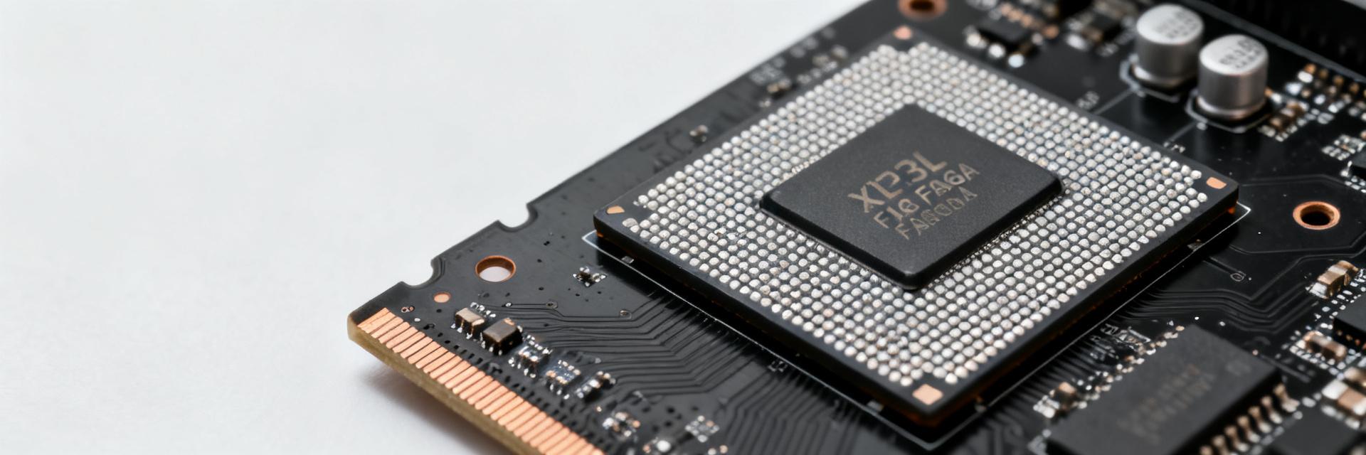
Key electrical & package highlights
| Spec | Value |
|---|---|
| Density / Organization | 2 Gbit / 128M x 16 |
| Nominal VDD / VDDQ | 1.35 V (DDR3L) |
| Max clock | 800 MHz input / DDR3-1600 effective |
| Typical CAS / access | CL ~11 (typical), ~13.75 ns effective access |
| Package | FBGA96-style |
| Temp range | Commercial/industrial options (check datasheet) |
The MT41K128M16JT-125 specification table above emphasizes the attributes engineers must capture during BOM review and early thermal/power modeling. Density and organization determine the bus mapping and interleaving strategy, VDD/VDDQ governs regulator selection and sequencing, and max clock defines the PHY timing envelope for signal integrity and layout constraints.
Who should pick this part (target applications)
This DDR3L part is well-suited to embedded systems, networking modules, industrial controllers, and any design constrained by lower supply voltage but requiring moderate bandwidth from a parallel SDRAM interface. Choose it when you need 2 Gbit density with a x16 data width and can accommodate FBGA footprint and the DDR3 signaling stack.
Rule of thumb: if your system needs a low-voltage DDR3 footprint with reliable sequential throughput around DDR3-1600 and an architecture that benefits from x16 width, this part is a sensible default choice.
2 — Electrical and timing deep-dive for MT41K128M16JT-125 (Data analysis)
Power, voltage ranges, and implications for power rails
VDD and VDDQ nominally target 1.35 V with allowed margins in the datasheet; standby and active currents vary by operating frequency and temperature. Read the datasheet’s Idd spec tables carefully: standby Idd2N/Idd3N constraints determine retention-mode budgeting while active Idd values at the target frequency set worst-case power draw. For thermal budgets, multiply active current by VDD to estimate dynamic power and add static leakage for hot-case estimates.
Worked example: at DDR3-1600, assume active Idd ≈ 150 mA (per-bank scaled example) on a single 128Mx16 device; dynamic power ≈ 1.35 V × 0.15 A = 0.2025 W. Multiply by population count and add regulator inefficiency (≈90%) to size power rails. The 1.35 V DDR3L benefit versus 1.5 V DDR3 yields ≈10% savings in dynamic power—valuable for battery or thermally tight boards.
Timing parameters and read/write latency trade-offs
Primary timing fields—CAS (CL), tRCD, tRP, and tRAS—combine with clock period to produce absolute latencies. At 800 MHz input (0.625 ns half-cycle; 1.25 ns full-cycle), a CL11 setting implies ~13.75 ns CAS latency; increasing frequency without adjusting CL raises cycle counts or absolute ns depending on controller settings. Effective throughput benefits from higher frequency, but random-access patterns amplify latency costs.
Recommendation: prioritize conservative timing (e.g., CL11–CL13 depending on margin) during bring-up, then tune toward tighter CAS if SI and temperature margins verify stability. Trade reliability for peak throughput only after interleaving and controller arbitration are validated.
3 — Performance benchmarks & real-world throughput (Data analysis)
Synthetic throughput and bandwidth expectations
Theoretical peak bandwidth for a single x16 DDR3-1600 device = 1600 MT/s × 16 bits = 25,600 Mbit/s = 3.2 GB/s. Real sustained throughput depends on access pattern: long sequential bursts approach peak, while random small transfers drop to a fraction due to precharge/activate overhead. Datasheet-derived tests should report read/write BW and latency percentiles to set system expectations.
Example: a sustained sequential read with 8-beat bursts and bank hits can achieve >70% of peak (~2.2 GB/s), while random 64B reads across banks may only realize 10–25% depending on controller arbitration and queue depth. Use burst-oriented benchmarks and percentile latency reporting for meaningful comparisons.
System-level bottlenecks and tips to maximize performance
Common bottlenecks include controller bandwidth limits, narrow external bus widths, poor bank utilization, and SI-induced errors at higher speeds. Address these with proper PHY/controller settings, enabling bank interleaving, and ensuring sufficient command/response queue depth in firmware. Monitor bank conflict rates and command timing statistics during validation.
Checklist: 1) validate PHY training and DLL locking; 2) enable bank interleaving and large burst sizes where possible; 3) measure and minimize byte-lane skew; 4) tune controller refresh scheduling to avoid throughput spikes.
4 — Integration checklist: PCB, SI, and firmware considerations (Method guide)
PCB layout and signal-integrity musts
Implement controlled-impedance routing for address/command and data lines (typically 50 Ω single-ended, 100 Ω differential where applicable), strict length-matching per byte lane (rule-of-thumb ≤ 50 ps skew), and matched stub avoidance. Termination schemes (RTT, ODT settings) should align with controller recommendations; decouple VDD and VDDQ near the FBGA with multiple MLCCs and power islands for thermal spreading.
Firmware/controller setup and validation steps
Initialization sequence: enforce correct VDD/VTT sequencing, run PHY training and impedance calibration, apply timing tables from validated board-config, and lock ODT/RTT. Validation tests include memory walk, checkerboard, pseudo-random patterns, long-running stress with continuous refresh, and throughput sweep at target frequencies/CL settings.
Recommended vectors: address walking, 32/64/128-bit stride accesses, long bursts to probe ODT behavior, and randomized read/write mixes to exercise arbitration. Log error rates, retry counts, and timing margins to document stability.
5 — Sourcing, alternatives, and recommended next steps (Action & case)
Comparable part classes and when to choose alternatives
Alternatives include x8 or x4 organizations and different density DDR3L variants. x8 parts reduce routing complexity and may better match 64-bit system buses, while x4 enables ECC configurations or higher effective banking. Trade-offs: x16 gives wider native bus per device but increases routing width and potentially area; x8 offers a middle ground for many embedded applications.
Choose the MT41K128M16JT-125 when low-voltage operation, x16 width, and FBGA footprint match system constraints; opt for x8/x4 if bus width, ECC, or footprint/cost pressures dominate.
Procurement checklist & deployment actions
Next steps: validate footprint against the chosen assembly house, request samples/evaluation devices, run power and timing validations across worst-case temperatures, and confirm supplier lead times for production. Update BOM with exact device marking and alternate sources to mitigate supply risk.
- Pre-launch test checklist: 1) footprint verification and DRC, 2) power-rail/load validation, 3) PHY training stability, 4) throughput/stress runs, 5) thermal soak and margin tests.
Summary
- The MT41K128M16JT-125 provides 2 Gbit (128M x 16) low-voltage DDR3L operation up to DDR3-1600, delivering ~3.2 GB/s theoretical bandwidth and favorable power for thermally constrained systems; verify regulator and sequencing for reliable operation.
- Top integration risks are SI at high speed, bank-conflict-induced latency, and insufficient PHY/controller tuning; prioritize length-matching, ODT configuration, and bank interleaving during bring-up.
- Immediate next steps: secure evaluation samples, run the recommended power and timing validation suite, and document results in the project validation log for cross-team review.