TC58BVG0S3HTA00 Specs Report: Pinout, Voltages, Timing
The TC58BVG0S3HTA00 belongs to the single‑chip 1 Gbit parallel NAND class used for raw flash storage in embedded controllers, boot devices, and industrial logging systems. These devices typically operate in the 3.3 V class and come in 48‑pin packages; accurate pinout, voltage and timing data are critical to avoid corruption, excessive current draw, or device damage.
This report gives concise, test‑oriented guidance so hardware and firmware engineers can validate rails, map pins correctly, set reliable timing margins, and perform first‑time bring‑up and debugging on target boards.
Background: Device overview and key identifiers
What the TC58BVG0S3HTA00 is and where it fits
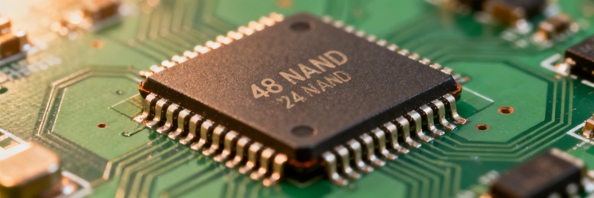
Technically, this part is a 1 Gbit NAND organized as 128M × 8 with an asynchronous parallel NAND interface and 3.3 V class supply expectations. Physically it is supplied in a 48‑pin small outline style package where power and ground pins are distributed for thermal and current handling. When checking specs, look for density (1 Gbit), I/O width (x8), package pin count and the presence of CLE/ALE/CE#/WE#/RE#/R/B# control signals to confirm the device family and capabilities.
Key electrical specs & pinout
Supply voltages, current, and absolute limits
Nominal operating VCC for this class is centered at 3.3 V; a safe recommended operating range is typically VCC = 2.7–3.6 V with VSS = 0 V. I/O supply (VCCQ or VCCIO where used) follows the same class unless the system implements a separate I/O rail. Active read/program currents commonly peak in the tens to low hundreds of milliamps during program/erase pulses; standby/hold currents fall to microamp or low‑milliamp ranges. Absolute maximum ratings usually specify input pin clamps and VCC max near 4.6 V and undershoot/ESD limits that require board ESD protection and controlled soldering profiles. Test conditions referenced here assume VCC = 3.3 V and 25°C ambient; always validate currents and thresholds on your system over full temperature range and with real load patterns.
| Parameter | Symbol | Min / Typ Value | Max / Limit |
|---|---|---|---|
| Operating Supply Voltage | VCC | 2.7 V | 3.6 V |
| Active Read/Program Current | ICC1 / ICC2 | — | 30 mA |
| Standby Current | ISB | — | 50 µA |
| Page Program Time | tPROG | 300 µs | 700 µs |
| Block Erase Time | tBERS | 2 ms | 10 ms |
Pinout map: pins, signals, and recommended usage
Group pins as: power (VCC, VSS) — place multiple VCC/VSS pins on separate decoupling nets; data/address bus (I/O0–I/O7, A0–An) — I/O lines are bidirectional and need short, equalized traces; command/control (CLE, ALE, CE#, RE#, WE#, R/B#) — CLE/ALE are inputs for command/address latching, CE# must never be left floating and usually needs a pull‑up, R/B# is an open‑drain ready/busy output and should have a pull‑up to VCC. Recommended pull values: small pull‑ups (10 kΩ–100 kΩ) for R/B# or CE# as a fallback, but actively drive timing‑sensitive control pins. Common package pin numbering places VCC pins spaced to minimize resistance; treat the package as a 48‑pin TSOP style with multiple ground pins for solid returns.
Timing and performance characteristics
Read/write/page timing overview
Key timing parameters to track include tR (data output access after read command), tWC/tWH (WE cycle and pulse widths), tPROG (page program time), and tBERS (block erase time). Typical test conditions are VCC = 3.3 V, 25°C. Example order‑of‑magnitude figures for similar 1 Gbit parallel NAND: tPROG in the sub‑millisecond to low‑millisecond range per page (e.g., ~0.7–2 ms), tBERS in the low‑millisecond range per block, and data‑bus access/RE# toggling measured in tens to hundreds of nanoseconds for burst window vs. longer latencies for initial page reads. Apply conservative margins: allow 1.5–2× the nominal program/erase times for reliable firmware state machines and calculate throughput accordingly (e.g., sustained page program throughput = page size / effective tPROG including overhead).
Command sequence and protocol notes
Essential sequences use CLE to latch commands, ALE to latch address cycles, and WE#/RE# to strobe; CE# must be asserted low to enable the device. Typical operations: send command via CLE, present address via ALE, then issue program/confirm commands and poll R/B#. For read operations, issue read command + column/page addresses, wait tR or poll R/B# then toggle RE# to clock data out. Use status reads after program/erase to detect errors; if R/B# stays busy beyond expected tPROG/tBERS margins, assert a timeout and retry with extended wait or block retire. Keep sequencing deterministic—avoid overlapping WE#/RE# pulses—and insert minimal guard times recommended for safe transitions.
Integration guide: power, decoupling, PCB layout & interface
Powering and decoupling best practices
Use a combination of bulk and local decoupling: 4.7–10 µF bulk cap per device rail plus 0.1 µF and 0.01 µF high‑frequency ceramics at each VCC pin. Place the smallest HF caps within 1–2 mm of the pin with direct vias to the ground plane. If separate VCCIO exists, ensure correct power sequencing so I/O never exceeds device VCC. Add a ferrite bead or series resistor on the VCC feed in noisy environments and consider a supervisor/reset IC to prevent undervoltage during power transitions. Thermal pads and copper pours under the package help dissipate program/erase heat in heavy write workloads.
PCB layout and signal integrity for the parallel interface
Route data/address lines as parallel, closely spaced traces over a continuous ground plane to keep impedance stable; avoid stubs longer than a few millimeters. For data bus buses, keep trace lengths matched within one or two propagation delays to avoid skew on multi‑bit transfers. Isolate high‑speed control nets from noisy power switching domains and add series resistors (22–47 Ω) on WE#/RE# or CE# if ringing is observed. Provide dedicated test points for CE#, R/B#, CLE/ALE and key I/O lines to simplify bring‑up and oscilloscope probing.
Validation, troubleshooting and practical checks
Test checklist for first-power-up and bring-up
Stepwise bring‑up: verify unloaded rails at board power‑on (VCC = 3.3 V ±10%), confirm VSS continuity and absence of shorts, assert/measure CE# pulled high when idle, monitor R/B# for defined idle state, then perform a simple ID/status read and read of factory page to confirm data path. Measure idle and active currents—expect microamp to low‑milliamp idle and tens of mA active; abnormal high currents indicate wiring errors or VCC mis‑levels. Use controlled power sequencing and a current limit supply on initial tests to prevent device or board damage.
Common failure modes and debugging tips
Typical symptoms: intermittent read errors often trace to poor decoupling or ground return impedance; corruption and unpredictable status often signal wrong supply voltage or swapped I/O lines in the pinout; persistent busy states imply timing margin violations or missing command sequences. Debug with an oscilloscope: capture CLE/ALE/WE#/RE# timing and inspect R/B# transitions. Fixes include adding local decoupling, increasing timing delays in firmware, verifying pinout wiring against the package pin map, and isolating suspect nets with series resistors or ferrite beads. When checking specs or pinout mismatches, confirm pull‑up/pull‑down placements and that CE# is never left floating.
Conclusion
Correct operation hinges on three priorities: stay within recommended operating voltages and absolute limits, wire the pinout exactly (power, data/address, CLE/ALE, control pins and R/B#), and apply conservative timing margins for program/erase/read cycles. With the right decoupling and PCB practices, typical 1 Gbit parallel NAND devices behave reliably in embedded systems.
Next steps: validate rails and pin wiring at first power‑up, capture control timing on a scope, and follow a bring‑up checklist to confirm read/write paths; consult the official device datasheet for full tables and absolute limits before production testing.
Key summary
- Device class: 1 Gbit, 128M × 8 parallel NAND — ensure correct package pin mapping and I/O direction before board bring‑up.
- Power: recommended VCC range ≈ 2.7–3.6 V with local 0.1 µF and bulk 4.7 µF decoupling near pins; watch inrush and program/erase current spikes.
- Pinout & control: CLE/ALE for command/address, CE#/WE#/RE#/R/B# sequencing must be deterministic; never float CE# or time‑sensitive inputs.
- Timing: provision margins for tPROG/tBERS (ms class) and bus access latencies; use polling of R/B# with safe timeouts to avoid hangs.
Common questions
How do I verify the device power rails during initial bring‑up?
Measure unloaded rails on a bench supply set to the recommended nominal (3.3 V). Check for shorts (VCC to VSS), then power with a current‑limited supply. Probe VCC at package pins and at decoupling caps; confirm local 0.1 µF and bulk caps are present and that inrush does not trip the source. Expected idle currents are low; significant milliamps before initialization suggest a wiring fault.
What is the recommended approach to detect and recover from program/erase timeouts?
Implement software timeouts longer than the nominal tPROG/tBERS (e.g., 1.5–2× nominal) and poll R/B# for ready status. On persistent busy, issue a status read to check failure flags, retry the operation a limited number of times, and mark the block bad if errors persist. Capture timing with a scope to distinguish device busy vs. misplaced control signals.
Which oscilloscope checkpoints are most useful for debugging read/write errors?
Probe CLE/ALE to confirm command/address strobing, WE#/RE# pulses for correct width and spacing, CE# to ensure device enabled state, and R/B# for ready/busy transitions. Also capture the I/O data lines during a read to check bit alignment and signal integrity. Use a low‑capacitance probe and ground spring to avoid corrupting the signals you are measuring.
Why must the CE# and R/B# pins be configured with pull-up resistors?
CE# must never be left floating to prevent accidental device selection or noise-induced activation during power transitions. R/B# is an open-drain output that requires an active external pull-up (typically 10 kΩ to 100 kΩ) to return to a high-logic state when the device becomes ready.