W25Q128JVSIQ Specs & Benchmark Breakdown — Latest Insights
The W25Q128JVSIQ is a 128M‑bit serial NOR device commonly chosen for compact code and data storage in embedded systems. Engineers evaluate it for boot, code XIP, and logging based on measurable specs and repeatable benchmark practices. This article distills device characteristics, practical test plans, and integration guidance so teams can validate suitability before production sign‑off.
1 — Quick overview & key specs (background)
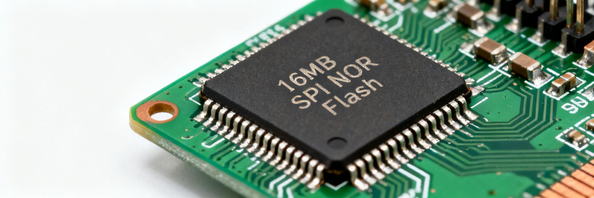
This section summarizes capacity, supply, and package details engineers reference during selection. The device presents 128M‑bit (≈16MB) density, a typical supply window around 2.7–3.6 V, and multiple small‑footprint packages suited for constrained PCBs. Designers should confirm package code and pinout on the received datasheet and log the device marking against the purchase order.
| Parameter | Specification Value | Operational Conditions / Notes |
|---|---|---|
| Memory Density | 128M-bit (16 Megabytes) | Structured in 65,536 programmable pages (256 bytes each) |
| Operating Voltage | 2.7V to 3.6V | Single supply source, typical 3.3V application standard |
| Max Clock Speed | 133 MHz | Supports Standard, Dual SPI, and Quad SPI physical modes |
| Package Code / Body | SOIC-8 (208-mil) | Standard package designator "SI" (SOIC-8 208mil) |
| Operating Temp | -40°C to +85°C | Industrial grade operating limits for core silicon stability |
Physical & electrical specifications
Point: The core physical and electrical specs determine board-level compatibility. Evidence: 128M‑bit capacity (≈16MB), common operating voltage 2.7–3.6 V, and compact packages with standard QSPI pinouts. Explanation: These specs drive decoupling, level‑translation needs, and PCB routing; verify VCC tolerance and recommended decoupling values during first article inspection to avoid margin issues in system power sequencing.
Memory organization & addressing
Point: Understanding page/sector/block layout informs erase/program strategies. Evidence: Typical page = 256 bytes, sector = 4 KB, large block = 64 KB; total pages ≈ 65,536 for 16 MB. Explanation: Use page‑aligned writes and sector/block erase granularity in firmware to minimize wasted cycles; include addressing examples in validation scripts to ensure correct offset math for bootloader and image storage.
2 — Architecture & reliability characteristics (data analysis)
Read/write/erase primitives & timings
Point: Command set and internal architecture set practical latency limits. Evidence: Devices support single, fast, dual, and quad read opcodes with dummy cycles and page program flows where program times vary by payload and sequence. Explanation: Measure read latency across modes and clock rates; record page program and block erase median/95th‑percentile times to size firmware timeouts and OTA update windows accurately.
Endurance, retention & environmental limits
Point: Lifecycle ratings guide acceptance criteria. Evidence: Typical program/erase endurance is on the order of 100k cycles with data retention spanning years under specified temperature limits and proper voltages. Explanation: Define lifecycle tests (e.g., accelerated P/E cycling to target statistical confidence and retention soak at elevated temperatures) and capture error modes like stuck bits and increased program time as failure indicators.
3 — Benchmark methodology & test setup (data analysis / benchmark)
Repeatable test plan & measurement metrics
Point: A repeatable benchmark plan isolates device behavior from host limitations. Evidence: Test across supported clock rates and SPI modes (single/dual/quad), varying transfer sizes and measuring throughput, command latency, and power. Explanation: Use a controller with known headroom, log bus timing and dummy cycles, and script tests to capture sustained throughput and per‑transaction latency so results are reproducible across lots.
Interpreting results & pitfalls to avoid
Point: Normalizing results avoids false conclusions. Evidence: Throughput scales with clock and effective bus width; caching, host driver, or DMA limits can mask device potential. Explanation: Normalize metrics by master clock and account for dummy cycles, present latency percentiles, and include host CPU load so that a low measured value can be traced to bus or firmware bottlenecks rather than the flash device itself.
4 — Integration & firmware optimization (method guide)
Bus configuration, timing tuning & command sequences
Point: Practical tuning increases effective throughput and stability. Evidence: Reducing dummy cycles where signal integrity allows and selecting the proper read opcode improves throughput; CS timing and drive strength affect margin. Explanation: Implement stepwise frequency ramp tests on representative boards, validate with stress scripts, and lock tolerances in firmware to avoid intermittent failures in marginal layouts.
Filesystem, wear management & XIP considerations
Point: Storage model affects endurance and responsiveness. Evidence: Using direct XIP reduces RAM cost but relies on steady read latency; filesystems add wear‑leveling for frequent updates. Explanation: Choose XIP for mostly–read firmware, add a small RAM cache for random writes, and deploy lightweight wear‑leveling or a flash translation layer when storing frequently updated telemetry to extend lifecycle.
5 — Comparative cases & real-world use cases (case showcase)
Typical embedded use cases & performance tradeoffs
Point: Different tasks impose distinct requirements. Evidence: Boot/firmware storage needs deterministic small‑read latency; XIP favors sequential execute speed; logging focuses on write/erase latency and endurance. Explanation: Map each use case to measurable requirements (read speed for boot, erase time for OTA, endurance for logging) and select operating points based on benchmarked numbers collected from representative boards.
Example integrations & measured outcomes
Point: Measurement drives design decisions. Evidence: In a typical MCU boot scenario, capturing command latency and first‑page read time predicts boot time; for OTA, block erase plus program throughput determines update duration. Explanation: Capture these benchmark numbers during validation to set user‑visible expectations and gating criteria for firmware rollouts and field updates.
6 — Procurement, validation & deployment checklist (action advice)
Datasheet & sample verification checklist
Point: Incoming verification prevents late surprises. Evidence: Confirm package marking, revision ID, and conformance to voltage/timing on the datasheet; run baseline throughput and page program tests per lot. Explanation: Keep a checklist that includes electrical checks, a minimal benchmark set (read throughput and program time), and counterfeit detection such as marking consistency and functional edge cases recorded during sample validation.
Production monitoring & lifecycle recommendations
Point: Field telemetry and production gates reduce escapes. Evidence: Define pass/fail thresholds for read throughput and erase/program times and collect telemetry on program failures, retries, and erase counts. Explanation: Implement production test gates that exercise key commands and log device identifiers; in the field, monitor retry rates and wear indicators to trigger maintenance or firmware mitigations.
Summary
- The W25Q128JVSIQ provides 128M‑bit (≈16MB) density with common supply range and standard page/sector/block organization; validate these specs during first article checks to confirm PCB and power compatibility.
- Benchmark plans should measure read/write/erase latencies across SPI modes and clock rates to distinguish device limits from host or board bottlenecks; use normalized metrics for comparisons.
- For boot and XIP prioritize deterministic small‑read latency; for logging emphasize endurance and erase time—run the outlined test checklist before production sign‑off to reduce field risk.
Frequently Asked Questions
What are the recommended test steps to validate W25Q128JVSIQ for boot use?
Validate boot use by measuring first‑page read latency at the intended clock and mode (single/quad), ensuring read margin across temperature, and confirming deterministic latency under system CPU load. Include power‑cycle and cold‑boot tests and log failure modes to set firmware retries and timeout thresholds.
How does W25Q128JVSIQ endurance affect filesystem and logging choices?
Assess endurance by planning expected update frequency against typical program/erase ratings. For frequent small writes, implement wear‑leveling or a journaling filesystem to spread wear across sectors. Where possible, batch writes and use an intermediate cache to reduce P/E cycles and extend field life.
Which benchmark metrics best predict OTA update time for W25Q128JVSIQ?
Key metrics are block erase time, sustained program throughput, and total image size; measure erase time variability and program throughput under worst‑case thermal conditions. Summing median erase+program times gives a realistic OTA window for user experience planning and rollback strategy design.
What are the hardware layout implications of operating W25Q128JVSIQ at 133MHz?
At 133MHz, trace impedance match (typically 50 ohms) is critical. Keep QSPI traces short, match trace lengths to minimize skew, and place decoupling capacitors (0.1uF and 4.7uF) directly adjacent to the VCC pin to suppress high-frequency noise.